Printed Circuit Board (PCB) development is the stage that bridges the gap between design and manufacturing. It is where ideas on paper are refined into practical layouts, validated against performance requirements, and prepared as working prototypes. Without proper development, even the most innovative design risks failure in production or performance.
For companies, startups, and research innovators in Vadodara, PCB developing services provide the foundation for faster product launches, lower costs, and greater reliability. With industries like automation, automotive, medical devices, and consumer electronics thriving in the region, the demand for dependable PCB development has grown significantly.
PCB developing refers to the stage where schematics and initial designs are translated into functional printed circuit boards that can be tested and refined. It is not just about drawing traces or preparing layouts but about ensuring that every element of the design can withstand real-world applications.
This involves converting schematics into manufacturable layouts, selecting suitable materials for performance and durability, and validating the design to ensure there are no electrical, thermal, or mechanical issues. Prototype boards are often created at this stage to verify the performance of the circuit before moving toward full-scale manufacturing.
In short, PCB developing is the step that confirms whether your design is production-ready. It helps reduce risks, improves efficiency, and saves costs by catching errors early.
Many businesses underestimate the importance of proper PCB development, often rushing directly from design to manufacturing. This approach can lead to costly mistakes such as signal integrity issues, overheating, or components not fitting correctly on the board.
By investing in development, companies reduce the chances of recalls, product failures, or delayed launches. For startups, this is particularly important because the ability to bring a product to market quickly and confidently can make the difference between success and missed opportunities.
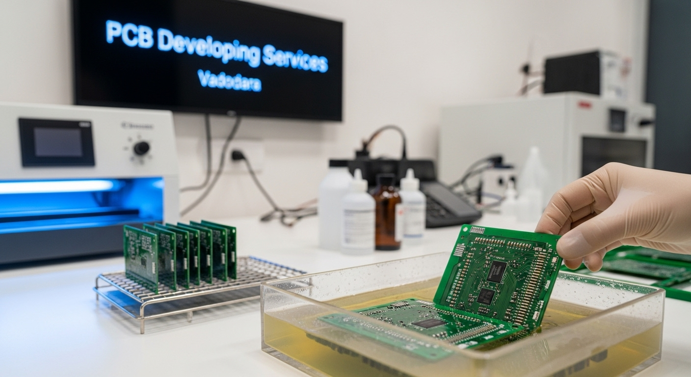
At Megabytes Circuit Systems, our PCB developing services are tailored to suit the unique requirements of each client. Whether you are working on a single-layer control board or a high-density multilayer design for advanced electronics, we provide end-to-end support.
Our capabilities include schematic capture and layout refinement, where we ensure that concepts translate into designs that can be efficiently manufactured. Material selection and stack-up planning are another critical aspect, as choosing between FR-4, polyimide, or advanced substrates can significantly affect the durability and performance of the final board.
We also carry out signal integrity and thermal analysis using advanced simulation tools, allowing us to predict how the board will perform under different conditions. This step is especially important for automotive, telecom, and medical applications where reliability is non-negotiable.
Once the design is validated, we move on to prototype development. By producing small-batch boards, we enable clients to test their circuits in real applications, make adjustments, and finalize the design before committing to mass production.
We follow a structured and transparent process to ensure quality results for every client.
The journey begins with requirement analysis, where we thoroughly understand the client’s goals, applications, and performance needs. From there, the schematic review allows us to identify potential issues or missing details before moving to the layout stage.
During layout optimization, our engineers refine routing, adjust trace widths, plan via placements, and balance the stack-up for signal integrity and thermal stability. Once layouts are finalized, prototype boards are created in limited numbers. These prototypes go through functional testing and validation to check whether the circuit behaves as expected in real-world conditions.
If adjustments are needed, refinements are made before the project moves to full-scale production. This disciplined process not only reduces risks but also ensures that the boards we deliver are aligned with both technical and commercial expectations.
Because we serve diverse industries, our team is experienced in adapting to specialized requirements, whether that means tighter tolerances, higher thermal resistance, or compliance with medical-grade standards.
Working with a local partner like Megabytes Circuit Systems provides multiple benefits. One of the biggest advantages is faster prototyping. With local facilities, delays due to long-distance shipping are eliminated, and projects move forward quickly.
Direct communication with our engineering team is another advantage, allowing clients to resolve issues or make changes without miscommunication. Local expertise also means we understand the specific needs of Vadodara’s industrial ecosystem and can provide solutions that align with local supply chains and resources.
Cost efficiency is another strong reason. By saving on logistics and avoiding repeated rework, businesses reduce overall development expenses while still receiving boards that meet international standards.
Our reputation as a trusted provider of PCB developing services in Vadodara is built on three pillars: expertise, technology, and commitment. Our engineers bring years of hands-on experience in PCB design, development, and validation. We use advanced Electronic Design Automation (EDA) tools and simulation software to detect flaws before they turn into expensive mistakes.
PCB projects often face challenges that, if ignored, can cause delays or failures. For instance, incorrect component footprints can result in assembly errors, while poor thermal design can lead to overheating in high-power circuits. High-frequency designs may experience signal interference, and incomplete documentation can slow down manufacturing.
At Megabytes Circuit Systems, we address these issues through rigorous validation processes. Our engineers use simulation-driven analysis to predict performance issues, check footprints against component libraries, and plan for thermal management from the start. Comprehensive documentation is prepared for each project, ensuring that manufacturers have everything they need for smooth production.
PCB design involves creating schematics and layouts, while developing focuses on refining, validating, and prototyping to ensure readiness for mass production.
Yes, we create small-batch prototypes that allow clients to validate performance before scaling up.
Absolutely. We work on single-layer boards as well as complex multilayer, high-density projects.
Yes. Our services are scalable, making them suitable for startups, research teams, and established enterprises.
pcb developing vadodara, pcb developing services vadodara, pcb development vadodara, pcb developing company vadodara, pcb developing manufacturers vadodara, pcb developing near me vadodara, pcb prototype developing vadodara, pcb board developing vadodara, pcb design and developing vadodara, pcb developing service provider vadodara, pcb developing process vadodara, pcb developing gujarat, pcb developing firm vadodara, pcb developing engineers vadodara, pcb developing prototyping vadodara, pcb developing electronics vadodara, pcb developing industry vadodara, pcb developing support vadodara, pcb developing fast turnaround vadodara, pcb developing professional vadodara, pcb developing for iot vadodara, pcb developing for medical devices vadodara, pcb developing for consumer electronics vadodara, pcb developing for automotive vadodara, pcb developing company gujarat, pcb developing expert vadodara, pcb developing startup support vadodara, pcb developing smt vadodara, pcb developing solutions vadodara, pcb developing outsourcing vadodara, pcb developing partner vadodara, pcb developing electronics gujarat, pcb developing affordable vadodara, pcb developing quick prototyping vadodara, pcb developing dfx vadodara, pcb developing turnkey vadodara, pcb developing trained engineers vadodara, pcb developing pcb manufacturer vadodara, pcb developing quality vadodara, pcb developing inspection vadodara, pcb developing assembly ready vadodara, pcb developing smt line vadodara, pcb developing pcb solutions vadodara, pcb developing smd vadodara, pcb developing contract vadodara, pcb developing prototype boards vadodara, pcb developing pcb fabrication vadodara, pcb developing pcb assembly vadodara, pcb developing functional testing vadodara, pcb developing startup vadodara, pcb developing local vadodara, pcb developing electronics near me vadodara.