Ahmedabad - 382430, Gujarat (India)
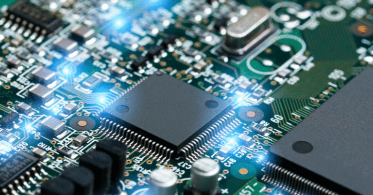
In the ever-evolving world of electronics, Double Layer PCBs (Printed Circuit Boards) have emerged as a fundamental component in the design and manufacturing of modern electronic devices. These boards, also known as double-sided printed circuit boards, feature conductive copper layers on both sides, connected through vias (plated holes), allowing for more complex and compact circuit designs.
Whether you’re an engineer designing advanced systems, a hobbyist working on a personal project, or a business developing electronic products, understanding the intricacies of double layer circuit boards is crucial. This comprehensive guide will delve into every aspect of Double Layer PCBs, from their design and manufacturing processes to their applications and advantages, providing you with the knowledge needed to make informed decisions for your projects.
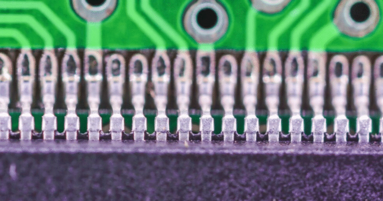
A Double Layer PCB is a type of printed circuit board that consists of two conductive copper layers, one on each side of the board. These layers are interconnected through vias, which are small holes drilled into the board and plated with conductive material, allowing electrical signals to pass between the two sides.
This dual-layer structure enables more complex circuit designs compared to single-layer boards, making double-sided PCBs a popular choice for a wide range of electronic applications.
The versatility of Double Layer PCBs lies in their ability to accommodate a higher density of components and provide better electrical performance. This makes them ideal for use in industries ranging from consumer electronics to automotive and aerospace.
For instance, double layer circuit boards are commonly found in smartphones, laptops, automotive control systems, and medical devices. Their compact design and improved performance have made them a cornerstone of modern electronics, bridging the gap between simple single-layer boards and complex multi-layer boards.
When considering the use of Double Layer PCBs for your project, it’s important to weigh their advantages and disadvantages to determine if they are the right fit for your needs.
One of the primary advantages of double-sided PCBs is their higher circuit density. With conductive layers on both sides of the board, these PCBs can accommodate more components and support more complex circuit designs.
This makes them ideal for applications where space is at a premium, such as in smartphones and wearable devices. Additionally, the dual-layer structure allows for a more compact design, enabling the creation of smaller and more lightweight electronic devices.
Another significant advantage of Double Layer PCBs is their improved electrical performance. The presence of two conductive layers allows for better signal integrity and reduced electromagnetic interference (EMI), which is crucial for high-frequency applications.
This makes double layer circuit boards suitable for use in advanced electronic systems, such as communication devices and industrial control systems.
Cost-effectiveness is another key benefit of Double Layer PCBs. While they are more expensive than single-layer boards, they are significantly more affordable than multi-layer boards.
This makes them an excellent choice for mid-complexity projects that require more functionality than a single-layer board can provide but do not justify the cost of a multi-layer board.
Furthermore, double-sided PCBs offer greater design flexibility, allowing engineers to create more innovative and efficient circuit layouts.
Despite their many advantages, Double Layer PCBs also have some drawbacks that need to be considered.
One of the main challenges is the complexity of the design process. Designing a double layer PCB requires careful planning to ensure proper via placement and avoid signal interference. This can be particularly challenging for engineers who are new to PCB design or working on highly complex circuits.
Another disadvantage is the higher cost compared to single-layer boards. While double-sided PCBs are more cost-effective than multi-layer boards, they are still more expensive to produce than single-layer alternatives.
This can be a limiting factor for projects with tight budgets. Additionally, the manufacturing process for double layer circuit boards is more complex, requiring precise drilling and plating for vias.
This can lead to longer production times and higher costs, especially for small-scale production runs.
Designing a Double Layer PCB requires a thorough understanding of electrical engineering principles and careful attention to detail. Here are some key considerations to keep in mind during the design process:
The arrangement of the top and bottom layers is crucial for ensuring optimal performance. Proper layer stackup helps minimize interference and improve signal integrity. For example, placing a ground plane on one side of the board can help reduce noise and provide a stable reference for signal routing. It’s also important to consider the thickness of the copper layers and the dielectric material between them, as these factors can impact the board’s electrical properties.
The placement of components on a double Sided PCB plays a significant role in the board’s performance. High-frequency components should be placed on one side of the board to minimize signal loss and interference. Additionally, adequate spacing between components is essential to prevent overheating and ensure reliable operation. Careful consideration should also be given to the placement of vias, as they can affect the routing of traces and the overall layout of the board.
The routing of traces on a double layer PCB is another critical aspect of the design process. Appropriate trace widths must be used to handle the current load and prevent overheating. Sharp angles in traces should be avoided, as they can cause signal reflection and degrade performance. Instead, use smooth curves or 45-degree angles to ensure optimal signal flow.
Vias are essential for connecting the two layers of a double layer PCB, but their placement must be carefully planned to avoid disrupting the circuit. Through-hole vias are commonly used for reliable connections, but blind and buried vias can also be employed in more complex designs. It’s important to ensure that vias are placed in areas that do not interfere with the routing of traces or the placement of components.
Effective thermal management is crucial for ensuring the reliability and longevity of a double layer PCB. Heat sinks and thermal vias can be used to dissipate heat and prevent overheating. It’s also important to avoid placing heat-sensitive components near high-power devices, as this can lead to thermal stress and potential failure.
The manufacturing process of double-sided printed circuit boards involves several steps to ensure precision and reliability. Here’s a detailed overview of the process:
The first step in manufacturing a double layer PCB is creating a schematic diagram of the circuit. This diagram is then converted into a PCB layout using specialized design software. The layout must be carefully verified for errors and optimized for manufacturing to ensure that the final product meets the required specifications.
The choice of materials is critical for the performance and durability of the PCB. The base material, typically FR-4, is selected for its excellent electrical insulation properties and mechanical strength. Copper foil is used for the conductive layers, with the thickness of the foil chosen based on the current requirements of the circuit.
The circuit design is printed onto the board using a photoresist process. A layer of photoresist material is applied to the copper foil, and the circuit pattern is transferred onto the board using UV light. The exposed areas of the photoresist are then developed, leaving behind the desired circuit pattern.
The next step is the etching process, where excess copper is removed from the board using a chemical solution. The photoresist protects the desired circuit traces, while the unwanted copper is dissolved, leaving behind the conductive pathways.
Holes are drilled into the board for vias and component leads. These holes are then plated with copper to create electrical connections between the two layers. The plating process ensures that the vias are conductive and provide reliable connections.
A solder mask is applied to the board to protect the copper traces and prevent short circuits. The solder mask is typically green, but other colors can be used for aesthetic or functional purposes. Openings in the solder mask are created for soldering components to the board.
Labels, component identifiers, and other markings are added to the board using silkscreen printing. This step helps with the assembly and troubleshooting of the PCB by providing clear identification of components and connections.
The final step in the manufacturing process is testing and quality control. Electrical tests are performed to ensure that the board functions as intended and meets the required specifications. The board is also inspected for defects, such as shorts, opens, or misaligned components, to ensure that it is ready for use.
Double Layer PCBs are used in a wide range of industries and applications, thanks to their versatility and performance. Here are some of the most common applications:
In the consumer electronics industry, double-sided PCBs are used in devices such as smartphones, tablets, and laptops. Their compact design and high circuit density make them ideal for these applications, where space is at a premium and performance is critical.
The automotive industry relies on double layer circuit boards for various applications, including engine control units (ECUs), infotainment systems, and LED lighting. The durability and reliability of these PCBs make them well-suited for the harsh environments found in vehicles.
In industrial settings, double layer PCBs are used in power supplies, control systems, and monitoring devices. Their ability to handle complex circuits and provide reliable performance makes them essential for industrial automation and control.
The medical industry uses double-sided PCBs in diagnostic equipment, imaging systems, and portable medical devices like glucose meters. The precision and reliability of these PCBs are crucial for ensuring the accuracy and safety of medical devices.
In the aerospace and defense industries, double layer PCBs are used in avionics systems, communication devices, and navigation systems. Their ability to withstand extreme conditions and provide reliable performance makes them ideal for these critical applications.
When choosing the right type of PCB for your project, it’s important to understand the differences between single-layer, double-layer, and multi-layer boards.
Single-layer PCBs are the simplest type of printed circuit board, featuring a single conductive layer on one side of the board. They are easy to design and manufacture, making them a cost-effective option for simple circuits. However, their limited circuit density and larger size make them unsuitable for more complex applications.
Double Layer PCBs offer a balance between simplicity and complexity, with two conductive layers that allow for more compact and efficient designs. They are more expensive than single-layer boards but provide better performance and higher circuit density. This makes them ideal for mid-complexity projects that require more functionality than a single-layer board can provide.
Multi-layer PCBs consist of three or more conductive layers, offering the highest circuit density and performance. They are used in advanced electronic systems where space and performance are critical. However, their complex design and manufacturing process make them significantly more expensive than single or double-layer boards.
Selecting the right manufacturer for your double layer PCB is crucial for ensuring the quality and reliability of your product. Here are some tips to help you make the right choice:
If you’re based in Ahmedabad, Gujarat, or anywhere in India, consider partnering with a local manufacturer who specializes in Double Layer PCBs. This can help reduce shipping costs and lead times while supporting local businesses.
Double Layer PCBs are a versatile and cost-effective solution for a wide range of electronic applications. By understanding their design, manufacturing process, and advantages, you can make informed decisions for your projects. Whether you’re developing consumer electronics, industrial equipment, or aerospace systems, double-sided printed circuit boards offer the perfect balance of performance and affordability.
If you’re looking for reliable Double Layer PCB manufacturing services in Ahmedabad, Gujarat, or across India, ensure you partner with a trusted manufacturer who can deliver high-quality boards tailored to your needs. With the right design and manufacturing partner, you can create innovative and efficient electronic devices that meet the demands of today’s fast-paced world.
C/10, Yogeshwar Estate, B/H Madhuram Estate, Nr. Vishala Estate, Sardar Patel Ring Rd, Odhav, Ahmedabad, Gujarat, Ahmedabad - 382430, Gujarat (India)
Copyright © 2025. Megabytes Circuit Systems All rights reserved.
Powered by FrogMEE Tech