Ahmedabad - 382430, Gujarat (India)
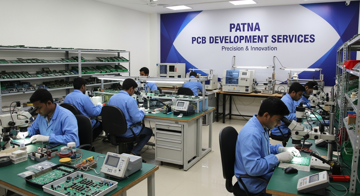
Patna, Bihar’s bustling capital and an emerging technology hub, is experiencing significant growth in electronics innovation, engineering education, and startup ecosystems. With prestigious institutions like IIT Patna, NIT Patna, and numerous engineering colleges producing talented graduates, the city has become a fertile ground for electronics development and hardware innovation.
As businesses ranging from startups to established manufacturers seek to transform ideas into functional electronic products, the demand for comprehensive PCB Developing Services in Patna has grown exponentially. Megabytes Circuit Systems delivers end-to-end circuit board development solutions that bridge the gap between concept and production-ready designs.
Our integrated approach combines schematic capture, PCB layout design, prototype fabrication, rigorous testing, and iterative refinement to ensure your electronic products meet performance specifications, regulatory requirements, and manufacturing feasibility standards. Whether you’re developing IoT devices, industrial controllers, consumer electronics, or specialized instrumentation, our PCB Developing Services in Patna provide the technical expertise and local accessibility that accelerate development timelines while controlling costs.
The electronics development landscape in Patna has transformed remarkably in recent years, driven by government initiatives promoting manufacturing, increased venture capital interest in regional innovation, and a growing pool of engineering talent.
Our PCB Developing Services in Patna support this vibrant ecosystem by providing professional development capabilities that were previously accessible only in major metropolitan areas. Local startups working on agricultural technology, healthcare devices, and smart city solutions benefit from having development partners who understand regional requirements and can provide rapid face-to-face collaboration when projects demand intensive technical discussions.
Established manufacturers expanding operations into Bihar discover that professional development services eliminate the trial-and-error approach that wastes time and resources. Instead, we provide methodical, proven development processes that progress efficiently from initial concept to validated designs.
The city’s strategic location, improving infrastructure, and cost advantages compared to larger metros make Patna an increasingly attractive destination for electronics manufacturing. Robust development services represent essential infrastructure supporting this growth.
Our approach to PCB Developing Services in Patna follows a systematic methodology refined through hundreds of successful projects across diverse industries and applications.
Development begins with requirement analysis sessions where our engineers work closely with you to understand:
This foundation ensures subsequent design decisions align with project objectives rather than requiring costly redesigns later.
Schematic design follows, translating system-level requirements into detailed circuit diagrams specifying components, interconnections, and electrical characteristics. Our PCB Design Service team performs comprehensive design reviews identifying potential issues before proceeding to the next phase.
PCB layout transforms schematics into manufacturable board designs where component placement, trace routing, power distribution, and signal integrity considerations are carefully optimized. Design rule checking and design-for-manufacturing analysis ensure layouts meet fabrication and assembly capabilities, preventing manufacturing issues that delay production.
Prototype fabrication produces initial boards for validation, followed by comprehensive testing verifying electrical performance, thermal behavior, electromagnetic compatibility, and functional operation. Our PCB Developing Services framework ensures all aspects receive proper engineering attention.
Our iterative refinement process addresses any issues discovered during testing, optimizing designs until they meet all specifications and are ready for volume manufacturing handoff.
Modern electronics development demands specialized knowledge across multiple engineering disciplines, and our PCB Developing Services in Patna provide access to expertise spanning analog circuits, digital systems, power electronics, RF communications, and embedded software integration.
High-speed digital designs operating at frequencies where signal integrity becomes critical receive careful attention to impedance control, transmission line effects, and electromagnetic interference mitigation.
Power supply circuits demanding precise voltage regulation, low noise, and high efficiency benefit from our experience with switching regulators, linear regulators, and power distribution network optimization.
Mixed-signal designs integrating sensitive analog circuits with digital processing require meticulous layout techniques separating noise sources from precision circuits while maintaining necessary interconnections.
For projects incorporating wireless communications, our RF expertise addresses antenna design, impedance matching, and regulatory compliance for various frequency bands and protocols.
Thermal management analysis ensures components remain within safe operating temperatures under worst-case conditions, incorporating appropriate heatsinking, thermal vias, and airflow considerations.
The versatility of our development capabilities enables us to serve remarkably diverse industry sectors, each presenting unique technical requirements and regulatory landscapes.
Medical device developers creating diagnostic equipment, patient monitoring systems, and therapeutic devices benefit from our understanding of biocompatibility requirements, electrical safety standards, and documentation practices supporting regulatory submissions.
Industrial automation companies designing programmable controllers, sensor networks, and machine interfaces rely on our experience with robust designs tolerating harsh electrical environments, temperature extremes, and mechanical vibration.
The agricultural technology sector, particularly relevant in Bihar’s agriculture-dependent economy, develops precision farming equipment, irrigation controllers, and crop monitoring systems requiring rugged designs optimized for outdoor deployment and minimal maintenance.
Educational institutions conducting electronics research leverage our development services to transform academic concepts into functional prototypes enabling further study and potential commercialization.
Consumer electronics manufacturers, renewable energy system developers, and telecommunications infrastructure providers all discover that professional development services dramatically reduce time-to-market while improving product reliability.
Today’s electronic products demand sophisticated PCB technologies beyond simple Single Layer PCB designs, and our PCB Developing Services in Patna encompass the full spectrum of modern board construction methods.
Double Layer PCB designs provide essential ground planes improving signal integrity and electromagnetic compatibility while accommodating moderate component densities suitable for many applications.
Multilayer PCB constructions with four, six, eight, or more layers enable complex high-density designs incorporating dedicated power and ground planes, controlled impedance signal routing, and intricate interconnection patterns impossible with simpler constructions.
Flexible PCB designs using polyimide or polyester substrates enable applications requiring board flexing or three-dimensional packaging impossible with rigid boards. Rigid-flex combinations integrate flexible interconnections with rigid circuit sections, eliminating connectors and cables while providing mechanical flexibility where needed.
High-frequency RF boards utilize specialized materials with precise dielectric constants and low loss tangents maintaining signal integrity at microwave frequencies. Metal-core PCBs with aluminum or copper substrates provide exceptional heat dissipation for power electronics and LED applications generating significant thermal energy.
HDI technologies incorporating microvias, fine-pitch features, and advanced buildup processes support miniaturized designs demanding maximum functionality in minimal space. Our development team selects appropriate technologies based on your application requirements, balancing performance needs against manufacturing complexity and cost considerations.
Speed represents a critical competitive advantage in technology markets, and our PCB Developing Services in Patna emphasize rapid development cycles that compress time-to-market without compromising design quality.
Our streamlined development process eliminates unnecessary delays, progressing projects through design stages efficiently while maintaining proper engineering rigor. Fast-track prototyping services deliver initial boards within days rather than weeks, enabling quick validation of critical design elements and early identification of issues requiring attention.
For urgent projects facing demonstration deadlines, trade show commitments, or unexpected competitive pressures, we provide expedited development services allocating additional engineering resources to accelerate schedules. Our PCB Calculator tool helps you quickly estimate costs and timelines for prototype quantities, facilitating rapid decision-making during planning phases.
Quick-turn iteration cycles address issues discovered during testing without lengthy delays, incorporating design refinements and producing updated prototypes rapidly. This iterative approach proves far more efficient than attempting perfect designs initially, as physical testing inevitably reveals real-world behaviors that simulation cannot fully predict.
Unlike distant development services requiring extended shipping times and communication delays, our Patna location enables rapid face-to-face meetings when complex technical discussions demand personal interaction, further accelerating development progress and ensuring clear understanding of requirements and solutions.
Comprehensive validation represents the foundation of successful product development, and our PCB Developing Services in Patna incorporate extensive testing protocols verifying designs meet specifications before committing to volume manufacturing.
Electrical testing begins with basic functionality verification ensuring circuits perform intended operations under nominal conditions. Performance characterization measures critical parameters across operating ranges, documenting actual behavior against design specifications and identifying any deviations requiring attention.
Stress testing applies extreme conditions—temperature ranges, voltage variations, loading scenarios—revealing design margins and potential failure modes. Environmental testing exposes prototypes to humidity, vibration, thermal cycling, and other conditions matching intended deployment environments, validating mechanical robustness and long-term reliability.
Electromagnetic compatibility testing measures both emissions generated by your device and susceptibility to external interference, ensuring compliance with regulatory limits and proper operation in electrically noisy environments. Safety testing for products connected to mains power or contacting users verifies appropriate isolation, grounding, and protective measures preventing electrical hazards.
For wireless devices, our testing includes antenna performance characterization, range validation, and coexistence testing with other wireless systems. This comprehensive validation approach identifies issues during development when corrections remain inexpensive, rather than discovering problems after production when remediation costs escalate dramatically.
Electronics development always involves trade-offs between performance, features, cost, and schedule, and our PCB Developing Services in Patna help clients navigate these decisions strategically.
Component selection significantly impacts both unit costs and development complexity, and we guide choices balancing performance requirements against pricing, availability, and supply chain considerations. Standardizing on commonly available components rather than exotic specialized parts reduces both procurement costs and supply chain risks.
Board technology selection appropriately matches design complexity to manufacturing capabilities, avoiding unnecessarily expensive constructions while ensuring adequate performance. Design-for-manufacturing optimization reduces fabrication and assembly costs by adhering to manufacturer capabilities rather than requiring specialized processes commanding premium pricing.
Volume projections influence design decisions, as investments in optimization delivering modest per-unit savings justify development costs only when multiplied across substantial production quantities. Make-versus-buy analysis determines which circuit functions warrant custom development versus utilizing commercial modules, balancing integration benefits against development costs and time investments.
Our transparent consulting approach presents options with honest assessments of trade-offs, enabling informed decisions aligned with business objectives rather than maximizing development service revenues. The result delivers maximum value from development investments, producing designs meeting technical requirements while remaining commercially viable.
We start with functional requirements describing what your product must accomplish, target specifications for key parameters, environmental conditions, physical constraints like size and weight limits, and anticipated production volumes. Existing documentation, reference designs, or preliminary sketches help but aren’t mandatory.
Timeline depends on complexity, but straightforward designs progress from requirements to validated prototypes within 4-6 weeks. Complex designs with extensive functionality, regulatory requirements, or cutting-edge technologies may require 2-3 months or longer for complete development and validation.
Absolutely. We frequently inherit partially completed designs requiring finishing, optimization, or troubleshooting. Our engineers review existing work, identify issues or gaps, and develop completion plans addressing remaining requirements efficiently.
Yes, upon project completion you receive complete design packages including schematic files, PCB layout files in industry-standard formats, bills of materials, assembly drawings, and fabrication specifications enabling manufacturing wherever you choose.
Design iteration is normal in development. We diagnose issues, develop solutions, and produce updated prototypes incorporating corrections. Our development proposals typically include contingency for reasonable iteration cycles addressing unexpected challenges.
We design circuits meeting relevant safety and EMC standards, prepare documentation supporting certification processes, and can coordinate with testing laboratories. While we don’t perform formal certification, our designs minimize compliance risks and certification costs.
Beginning your development journey with our PCB Developing Services in Patna follows a collaborative process designed to establish clear understanding and realistic expectations from the outset.
Initial consultation discusses your product vision, technical requirements, constraints, and objectives, allowing our team to assess project scope and identify potential challenges requiring attention. We prepare a detailed proposal outlining development approach, deliverables, timeline, and costs, ensuring alignment before work begins.
Upon approval, development proceeds through planned stages with regular progress reviews keeping you informed and providing opportunities for feedback and course corrections as understanding evolves. Our transparent communication philosophy means you receive honest assessments of progress, challenges, and solutions rather than discovering problems late in development cycles.
Throughout the project, you maintain ownership of intellectual property and design files, with all work product delivered upon completion. Beyond individual projects, many clients establish ongoing development partnerships as product lines expand and new projects emerge, benefiting from our accumulated understanding of their technical preferences, design standards, and business requirements.
This relationship-focused approach transforms transactional service provision into collaborative partnerships accelerating innovation and commercial success. Contact our team today to discuss your development requirements and discover how professional PCB development services can transform your product concepts into market-ready electronic devices. Our Patna-based engineering team is ready to bring your ideas to life with precision, expertise, and dedication to your success.
PCB Developing Services Patna, PCB Development Patna, Circuit Board Development Patna, PCB Design and Development Patna, Electronic Product Development Patna, PCB Engineering Services Patna, Custom PCB Development Patna, PCB Developer Patna, PCB Development Company Patna, PCB Development Services Patna Bihar, Hardware Development Patna, Circuit Design Services Patna, Schematic Design Patna, PCB Layout Design Patna, Prototype Development Patna, PCB Prototyping Patna, Product Design Services Patna, Electronics Design Patna, PCB Design Service Patna, PCB Design Engineer Patna, Professional PCB Development Patna, Expert PCB Developer Patna, Fast PCB Development Patna, Quick PCB Design Patna, Rapid Prototyping Patna, PCB Design Solutions Patna, Complete PCB Development Patna, End to End PCB Services Patna, Turnkey PCB Development Patna, PCB Consulting Services Patna, PCB Design Consultation Patna, Hardware Engineering Patna, Embedded Systems Development Patna, IoT Hardware Development Patna, Industrial PCB Design Patna, Medical Device PCB Patna, Automotive PCB Development Patna, Consumer Electronics Design Patna, RF PCB Design Patna, High Speed PCB Design Patna, Power Electronics Design Patna, Analog Circuit Design Patna, Digital Circuit Design Patna, Mixed Signal PCB Design Patna, Multilayer PCB Design Patna, Flexible PCB Development Patna, Rigid Flex PCB Design Patna, HDI PCB Development Patna, PCB Testing Services Patna, Design Validation Patna, PCB Optimization Patna, Design for Manufacturing Patna, DFM Analysis Patna, PCB Reverse Engineering Patna, Circuit Redesign Patna, Legacy PCB Updates Patna, PCB Cost Reduction Patna, Affordable PCB Development Patna, Best PCB Developer Patna, Top PCB Design Company Patna, PCB Development Near Me, Local PCB Designer Patna, PCB Development Bihar, PCB Engineering Patna, Circuit Board Engineer Patna, Product Development Services Patna, Hardware Prototyping Patna, Concept to Production Patna, PCB Development Quote Patna
C/10, Yogeshwar Estate, B/H Madhuram Estate, Nr. Vishala Estate, Sardar Patel Ring Rd, Odhav, Ahmedabad, Gujarat, Ahmedabad - 382430, Gujarat (India)
Copyright © 2025. Megabytes Circuit Systems All rights reserved.
Powered by FrogMEE Tech