Ahmedabad - 382430, Gujarat (India)
The relentless push toward “smart everything” has forced hardware engineers to rethink the traditional boundaries of circuit design. In the IoT (Internet of Things) era, the primary challenge is no longer just connectivity it is space. Fitting a micro-controller, multiple sensors, a power management IC, and an RF antenna into a wearable or a compact industrial sensor requires a masterclass in small form factor pcb engineering.
For many Indian startups and developers, the jump to complex HDI (High-Density Interconnect) or high-layer count boards can be cost-prohibitive. This is where the optimization of double layer pcb india standards becomes critical. At Megabyte Circuit Systems, we specialize in helping engineers push the limits of two-layer designs to achieve miniaturization goals without the expense of multilayer fabrication.
Quick Technical Summary: Double-layer PCBs remain the preferred choice for IoT due to their cost-to-performance ratio and faster prototyping cycles. Miniaturization is achieved through high-density SMD placement and optimized routing techniques that maintain signal integrity on a two-layer FR4 substrate.
While a Multilayer PCB offers dedicated ground and power planes, the double layer pcb india market continues to grow because it offers a significant cost advantage for high-volume IoT nodes. The challenge, however, is dealing with EMI (Electromagnetic Interference) and thermal dissipation in a confined space without those dedicated planes.
To achieve a small form factor pcb, engineers are moving away from through-hole components and toward ultra-fine pitch SMD (Surface Mount Device) packages like WLCSP (Wafer Level Chip Scale Packaging) and QFN (Quad Flat No-leads). This shift requires a reliable pcb manufacturer capable of handling tighter trace width and clearance tolerances. At Megabyte, our PCB Manufacturing service is tuned to handle 4-mil traces, allowing for the dense routing required by modern ESP32, Nordic, or STM32-based IoT designs.
Quick Technical Summary: IoT DFM focuses on reducing via sizes and optimizing the solder mask to prevent defects in fine-pitch components. Implementing “Via-in-Pad” (where permissible) and minimizing annular rings are essential strategies for reclaiming valuable board real estate.
When designing a pcb prototype for iot, the DFM (Design for Manufacturing) rules you follow will determine the yield and reliability of your product. For miniaturized designs, we recommend several specific adjustments to your Gerber files:
If your internal team is struggling with these constraints, utilizing a professional PCB Design Service can help bridge the gap between a conceptual schematic and a manufacturable layout.
Understanding the trade-offs between layer counts is vital for procurement managers balancing performance and budget.
Feature | Double-Layer PCB | Multilayer PCB (4+ Layers) | Impact on IoT Design |
Cost | Lower (Best for BOM optimization) | Higher (Significant price jump) | Crucial for 10–\20 IoT nodes. |
Signal Integrity | Moderate (Requires careful routing) | Excellent (Dedicated GND planes) | Vital for high-speed WiFi/BLE. |
Size Constraints | Moderate | Excellent (Vertical density) | Multilayer allows for smaller X-Y dimensions. |
Manufacturing Time | 24-48 Hours (Quick-turn) | 4-7 Days | Critical for rapid PCB Developing Services. |
Thermal Mgmt | Limited (Requires thermal vias) | High (Internal planes act as sinks) | Important for cellular (LTE/5G) IoT. |
While a Single Layer PCB might work for a simple LED driver, the complexity of IoT pcb design almost always starts at the double-layer level to accommodate the necessary return paths for RF signals.
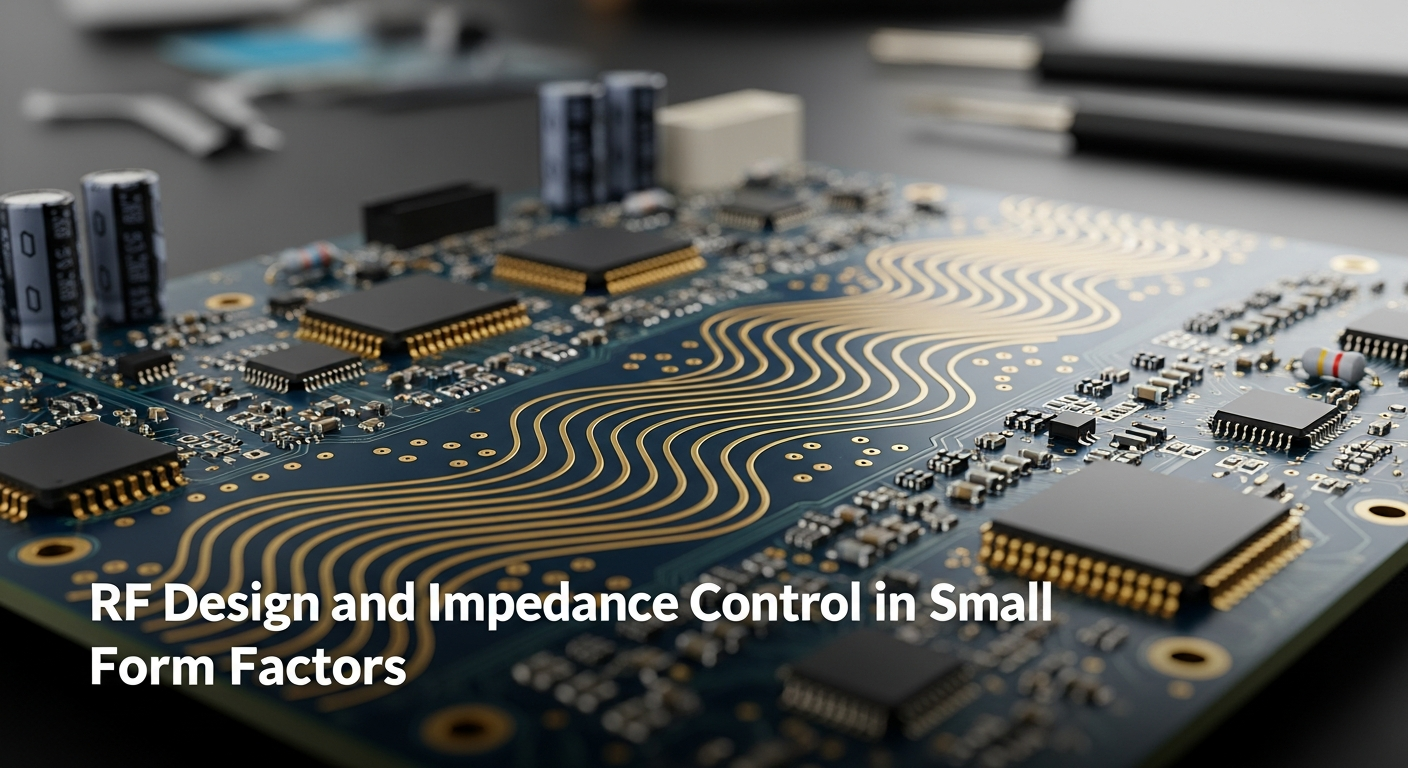
Quick Technical Summary: Managing RF impedance on a double-layer board requires precise substrate thickness selection and trace geometry calculations. Since there is no internal ground plane, the bottom layer must act as a reference to maintain the standard 50-ohm impedance required for IoT antennas.
In miniaturized IoT devices, the antenna is often the most sensitive component. Whether you are using a PCB trace antenna (like an Inverted-F) or a ceramic chip antenna, the feedline must be impedance-matched. On a double layer pcb india standard FR4 substrate, the trace width (w) for a 50Ω microstrip is determined by the height (h) of the dielectric.
The formula for characteristic impedance (Z0) is:
Z0=ϵr+1.4187ln(0.8w+t5.98h)
Where:
At Megabyte, we provide precise dielectric stack-ups so your calculations match the physical reality of the board. This precision is why we are considered a reliable pcb manufacturer for RF-intensive applications like LoRaWAN, Zigbee, and NB-IoT.
Quick Technical Summary: Quality control for small form factor PCBs involves high-resolution AOI and E-Testing to identify microscopic defects in fine-pitch traces. Megabyte utilizes Flying Probe testing to ensure 100% netlist integrity without the need for expensive test fixtures.
Miniaturization increases the risk of manufacturing defects. A 4-mil trace is more susceptible to “opens” caused by dust during the imaging process. To mitigate this, we employ:
Quick Technical Summary: To minimize costs, engineers should avoid “over-specifying” tolerances and use standard panel sizes provided by the fabricator. Leveraging an online calculator helps in visualizing the price impact of different surface finishes like HASL versus ENIG.
For many startups, the goal is to reach a “Price-to-Density” sweet spot. Here is how to optimize your costs at Megabyte:
Yes, but it requires extreme care. You must ensure a solid ground return path directly under high-speed signal traces. If your design exceeds 100MHz or has fast rise times, a 4-layer board is generally safer.
We typically support a minimum drill size of 0.2mm (8 mil) with a 0.4mm (16 mil) annular ring for standard production. For specialized IoT needs, contact us for tighter tolerances.
This is often due to poor ground plane continuity or interference from nearby switching power supplies. Ensure your antenna has a clear “keep-out” zone where no copper or components are present on any layer.
If you are using 0402 components or fine-pitch ICs, ENIG is highly recommended. It provides a flat surface for the PCB Assembly service, reducing the risk of tombstoning or cold solder joints.
Simply upload your Gerber files to our PCB Calculator. We offer instant pricing for most standard double-layer configurations.
Miniaturization is the engine of the IoT revolution, but it requires a fabrication partner that understands the technical nuances of high-density design. Whether you are at the PCB Design Service stage or ready for a full-scale production run, Megabyte Circuit Systems provides the engineering support and manufacturing precision to bring your vision to life.
Don’t let space constraints hold back your innovation. Leverage our expertise in double layer pcb india manufacturing to build smaller, smarter, and more cost-effective IoT solutions.
Ready to start?
C/10, Yogeshwar Estate, B/H Madhuram Estate, Nr. Vishala Estate, Sardar Patel Ring Rd, Odhav, Ahmedabad, Gujarat, Ahmedabad - 382430, Gujarat (India)
Copyright © 2025. Megabytes Circuit Systems All rights reserved.
Powered by FrogMEE Tech