Ahmedabad - 382430, Gujarat (India)

In my 20+ years of working on the factory floor at Megabyte Circuit Systems, I’ve seen countless hardware engineers and R&D managers agonize over board layouts, trace routing, and component selection, only to treat the PCB surface finish as an afterthought.
One thing I always tell my clients is this: your surface finish is the critical bridge between your bare board and your components. Choose the wrong finish, and you might end up with tombstoning, poor solder joint reliability, or a batch of boards that oxidize before they even reach the assembly line.
When you finalize your PCB design, you have to balance budget constraints, component pitch, and the intended shelf life of the bare boards. Whether you are scaling up a consumer IoT device or validating a high-reliability medical instrument, the finish you select directly impacts your manufacturing yield. As a senior consultant, I am going to break down the exact technical differences between HASL, Lead-Free HASL, ENIG, and OSP so you can make an informed, cost-effective decision for your next project.
A PCB surface finish protects exposed copper from oxidation and provides a solderable surface for component assembly. The right finish ensures optimal pad coplanarity, dictates the board’s maximum shelf life, and directly influences the reliability of the Intermetallic Compound (IMC) formed during reflow soldering.
Exposed copper naturally oxidizes when exposed to air. If your copper pads oxidize, solder will not wet properly during assembly, leading to cold solder joints and field failures. The surface finish acts as a protective barrier until the board passes through the reflow oven.
But it’s not just about rust prevention. As electronic components shrink, the flatness of your pads known as pad coplanarity becomes absolutely vital. A finish that is slightly uneven might be perfectly fine for standard through-hole resistors, but it will completely ruin the assembly of a fine-pitch Ball Grid Array (BGA).
Let’s dive into the four most common finishes we process at our Ahmedabad facility and look at exactly where each one shines.
HASL is a traditional, highly durable surface finish created by dipping the PCB in molten solder and using hot air knives to level it. While it offers excellent shelf life and low cost, its uneven surface topography makes it unsuitable for fine-pitch components and modern SMD layouts.
For decades, HASL was the undisputed king of the PCB industry. The process is straightforward: the fabricated board is submerged in a bath of molten tin-lead solder, and as it is pulled out, high-pressure hot air knives blow off the excess.
Because it uses actual solder, the wetting during assembly is phenomenal. If you are designing a rugged Single Layer PCB with large through-hole components like relays, transformers, or robust connectors, standard HASL is incredibly cost-effective and gives you a shelf life of over 12 months.
However, we see this issue very often with modern designs: the hot air leveling process leaves a slightly domed, uneven surface on the pads. If you try to place a fine-pitch microcontroller on a HASL pad, the chip will slide off or tilt during reflow. Therefore, I never recommend standard HASL for dense SMD layouts.
Lead-Free HASL replaces the traditional tin-lead alloy with a tin-copper-nickel (or similar) RoHS-compliant alternative. It retains the low cost and long shelf life of standard HASL but requires higher processing temperatures, which can induce thermal stress on the bare board.
When the RoHS (Restriction of Hazardous Substances) directive changed the global electronics landscape, Lead-Free HASL stepped up to replace the traditional tin-lead process. It operates on the exact same principle but uses lead-free alloys.
This is a fantastic, budget-friendly option if you are spinning up a standard Double Layer PCB for a smart home switch or a basic motor controller that doesn’t utilize ultra-fine pitch components.
The main technical tradeoff here is the melting point. Lead-free solder alloys require significantly higher temperatures in the dipping bath (often around $260^\circ C$ to $280^\circ C$). This puts higher thermal stress on your FR4 substrate. If your board is particularly thin or has aggressive cutouts, the intense heat of Lead-Free HASL can occasionally cause board warpage.
ENIG consists of a thin layer of gold over a thicker layer of electroless nickel, providing a perfectly flat surface ideal for BGA, CSP, and fine-pitch components. It offers exceptional oxidation resistance and wire bondability, making it the industry standard for high-density, complex electronics.
In my experience, ENIG is the gold standard—literally and figuratively. The process involves a chemical deposition of a nickel barrier layer, followed by a thin layer of immersion gold. The gold strictly serves to protect the nickel from oxidation; during the soldering process, the gold dissolves into the solder joint, and the actual bond is made with the nickel layer.
Standard thickness profiles for ENIG generally follow these parameters:
Why is ENIG so critical? Flatness. ENIG provides extreme pad coplanarity. If you are designing a high-speed Multilayer PCB heavily populated with FPGAs, BGAs, or QFN packages, ENIG is non-negotiable. The perfectly flat pads ensure that every tiny solder ball on a BGA makes equal contact, eliminating open circuits and bridging. It also boasts a massive shelf life (12+ months) and excellent resistance to environmental tarnishing. The only downside is the higher cost due to the complex chemical process and raw material prices.
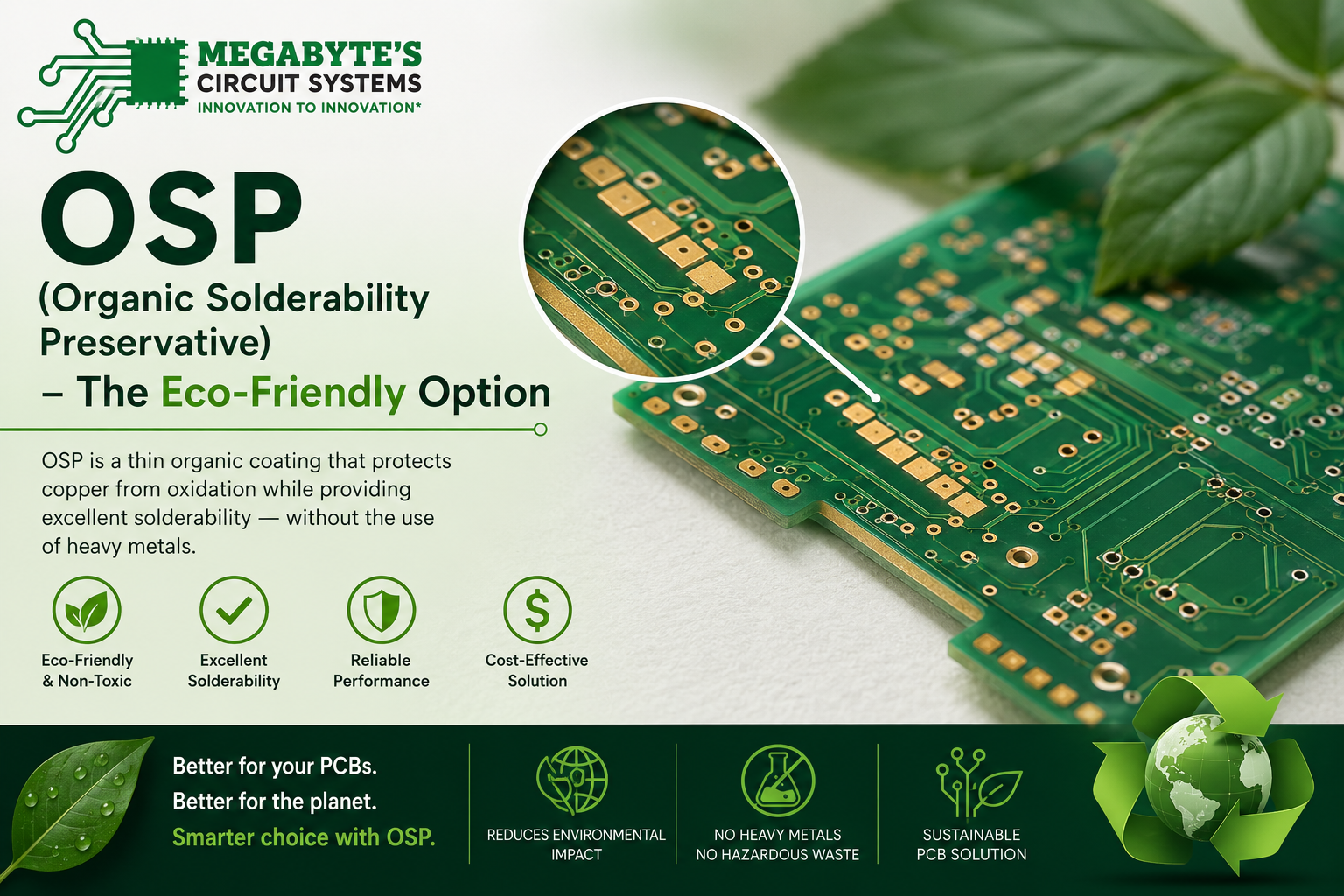
OSP is a water-based, organic compound applied over bare copper that protects it from oxidation prior to soldering. It provides a very flat surface at a low cost but has a limited shelf life and is highly sensitive to handling and multiple thermal cycles.
Unlike HASL or ENIG, OSP doesn’t add any metal to the copper pads. Instead, it uses a chemical compound to create a microscopic organic film over the exposed copper.
OSP is brilliant because it is cheap, environmentally friendly, and leaves the copper pads perfectly flat. However, it requires highly controlled inventory management. The organic film degrades over time and is highly sensitive to humidity, acidic oils from human fingerprints, and heat.
If you have a mixed-technology board that requires multiple trips through the reflow oven (e.g., top-side SMD, bottom-side SMD, then wave soldering), OSP can degrade before the final soldering stage. I generally advise clients to only use OSP if they know their bare boards will be assembled within 3 to 6 months of fabrication.
Selecting the right PCB surface finish requires balancing component pitch requirements against budget and shelf-life expectations. ENIG is the best overall performer for complex boards, while Lead-Free HASL offers the best cost-to-durability ratio for simpler designs.
Here is a quick reference matrix I use when consulting with procurement teams to help them match the finish to the project constraints:
Surface Finish | Pad Flatness / Coplanarity | Average Shelf Life | Relative Cost | RoHS Compliant | Best Used For |
HASL (Tin/Lead) | Poor (Uneven) | 12+ Months | Low | No | Through-hole, legacy military/aerospace |
Lead-Free HASL | Poor to Fair | 12+ Months | Low | Yes | General consumer electronics, standard SMD |
ENIG (Gold) | Excellent (Flat) | 12+ Months | High | Yes | BGAs, fine-pitch SMD, high-reliability devices |
OSP (Organic) | Excellent (Flat) | < 6 Months | Very Low | Yes | High-volume production, immediate assembly |
Different industries have completely different risk profiles. What works for a toy won’t work for a heart monitor. Here is how I usually guide our clients:
To optimize PCB fabrication costs in India, standardize your surface finishes across product lines to leverage volume pricing. Partnering with a domestic fabricator for advanced finishes like ENIG eliminates import duties and ensures stringent IPC-A-600 quality control.
A major part of my job is helping Indian R&D teams optimize their bills of materials. If you want to keep your prototype and production costs down, standardize your processes.
For instance, if your company designs both simple power supply boards and complex controller boards, don’t mix and match HASL and ENIG orders in small batches. Batching your advanced designs into a unified PCB Manufacturing service run with a single premium finish like ENIG can sometimes be more cost-effective overall due to reduced tooling and setup fees.
Furthermore, having your ENIG boards manufactured locally at our Ahmedabad facility ensures you don’t face the customs delays or heavy import duties associated with overseas suppliers. We monitor our chemical baths daily to prevent defects like “Black Pad” (a rare but severe nickel corrosion issue in ENIG), ensuring your boards meet strict IPC-A-600 standards.
I strongly advise against it. The uneven surface of HASL means some BGA solder balls will touch the pads while others hover slightly above them. During reflow, this causes bridging, open circuits, and incredibly weak joints that will fail in the field. Always use ENIG or OSP for BGA layouts.
OSP is an organic film that is highly sensitive to handling. If your assembly technicians are touching the bare boards without gloves, the acidic oils from their skin will dissolve the OSP layer, leading to rapid copper oxidation. OSP boards must be stored in vacuum-sealed bags with desiccants.
Yes, it does. The top layer is pure immersion gold. However, it is an incredibly thin layer (usually around $0.05 \mu m$ to $0.12 \mu m$). Its sole purpose is to protect the underlying nickel from oxidizing before the board is soldered.
Not always. While it offers the best performance for fine-pitch components, it is more expensive. If you are building a simple, double-sided through-hole board where cost is the primary driver, paying a premium for ENIG offers no functional advantage over Lead-Free HASL.
Yes. The hard gold surface of ENIG is highly conductive and holds up perfectly to the physical contact of flying probe testing needles without sustaining damage to the pads.
Choosing the right surface finish is a critical decision that bridges the gap between your CAD software and a physical, reliable product. Whether you need the budget-friendly durability of Lead-Free HASL for a rapid prototype, or the flawless coplanarity of ENIG for a complex IoT gateway, Megabyte Circuit Systems is equipped to deliver.
We pride ourselves on helping Indian engineers build world-class hardware without the headaches of overseas logistics. Now that you know exactly which finish your project needs, take the next step. Head over to our online PCB Calculator, enter your board dimensions, select your preferred surface finish, and instantly see how competitive our local manufacturing rates truly are.
Upload your Gerber files today, and let’s get your hardware built right.
C/10, Yogeshwar Estate, B/H Madhuram Estate, Nr. Vishala Estate, Sardar Patel Ring Rd, Odhav, Ahmedabad, Gujarat, Ahmedabad - 382430, Gujarat (India)
Copyright © 2025. Megabytes Circuit Systems All rights reserved.
Powered by FrogMEE Tech