Ahmedabad - 382430, Gujarat (India)
Printed Circuit Boards (PCBs) are the cornerstone of modern electronics, enabling everything from smartphones to satellite systems. At the heart of every PCB lies its layout a meticulously planned arrangement of components and electrical connections on a non-conductive board. The PCB layout is far more than a technical diagram; it’s a critical blueprint that determines a device’s performance, reliability, and manufacturability. A well-executed layout ensures seamless operation, while a flawed one can lead to costly failures. This guide explores the intricacies of PCB layout, from its fundamental principles to advanced applications, offering insights for hobbyists, engineers, and industry professionals alike.
In this comprehensive guide, we’ll dive into the materials, processes, and considerations that shape PCB layouts. You’ll learn about the design process, manufacturing steps, real-world applications, and emerging trends that are redefining the field. Whether you’re designing a simple prototype or a complex aerospace system, understanding PCB layout is essential to creating electronics that perform flawlessly.
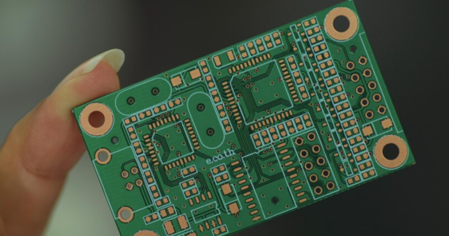
PCB layout is the art and science of arranging electronic components and their interconnections on a board made of insulating material, such as fiberglass or polyimide. It transforms an electrical schematic a conceptual diagram of how components connect into a physical structure that can be manufactured and assembled. The layout process requires balancing electrical performance, mechanical constraints, and thermal management to create a board that is functional, reliable, and cost-effective.
A successful PCB layout minimizes signal interference, optimizes heat dissipation, and ensures the board can be produced efficiently. It serves as the bridge between design and reality, guiding manufacturers through every step of fabrication and assembly. From consumer gadgets to mission-critical medical devices, the precision of the PCB layout directly impacts the success of the final product.
The choice of material is a foundational aspect of PCB layout, as it affects the board’s electrical properties, thermal behavior, and durability. Different materials are selected based on the application’s requirements, such as flexibility, heat dissipation, or high-frequency performance. Below are the most commonly used materials:
Each material brings unique advantages, and selecting the right one ensures the PCB meets the electrical, mechanical, and environmental demands of its intended use.
PCB layout is a convergence of electrical engineering, mechanical design, and manufacturing expertise. It must accommodate the circuit’s electrical needs such as signal integrity and power distribution while fitting within the mechanical constraints of the device’s size and shape. Additionally, the layout must align with manufacturing processes, ensuring the board can be produced efficiently and tested for quality.
The layout process generates critical documentation, including Gerber files (which define the board’s layers), drill files (specifying hole locations), and the Bill of Materials (BOM, listing components). These files guide manufacturers, minimizing errors and ensuring the final PCB matches the designer’s vision. A well-crafted layout enhances reliability, reduces production costs, and supports long-term performance.
Designing a PCB layout requires careful consideration of several factors, each influencing the board’s performance and manufacturability. Ignoring these can lead to signal issues, overheating, or production challenges. Key considerations include:
Balancing these factors requires expertise and often involves trade-offs. For example, a smaller board may save space but complicate thermal management. Design software helps engineers simulate and refine layouts to achieve the best outcome.
Creating a PCB layout is a structured process that transforms a schematic into a manufacturable board. Each step demands precision to ensure the final product meets its specifications.
The process begins with a schematic a logical diagram showing how components connect electrically. Created using software like Altium, KiCad, or Eagle, the schematic serves as the roadmap for the layout. It defines component relationships and helps identify potential errors, such as incorrect connections, before moving to the physical design.
Placing components is a critical step that affects signal integrity, thermal performance, and usability. High-frequency components, like RF modules, are positioned to minimize trace lengths and avoid interference. Power components require space for heatsinks or thermal vias. User-facing elements, such as connectors or buttons, must be accessible within the device’s enclosure. Design software allows engineers to experiment with placements, ensuring optimal performance.
Routing involves drawing copper traces to connect components, forming the circuit’s electrical pathways. Trace width and spacing are tailored to handle current loads and prevent short circuits. For high-speed signals, impedance matching and equal-length traces are crucial to avoid delays or noise. In multi-layer boards, vias connect traces across layers, requiring careful layer management to optimize space and performance.
Once the layout is finalized, Gerber files are generated. These files describe the board’s layers, including copper traces, solder masks, and silkscreen markings. Drill files specify hole locations, and the BOM lists all components. Accuracy is paramount, as errors in Gerber files can lead to defective boards. Most design software includes validation tools to catch issues before submission to manufacturers.
The PCB layout guides the manufacturing process, which transforms raw materials into a functional board. Each step requires precision to ensure the board matches the design.
The base material, such as FR-4 or polyimide, is cleaned to remove contaminants. A pristine surface ensures strong adhesion for copper layers and coatings, preventing defects during fabrication.
For high-frequency PCBs, a Teflon-based coating may be applied to reduce signal loss and enhance transmission. This step is common in RF and microwave applications, where low dielectric constants are critical.
Thin copper sheets are laminated onto the board, forming the conductive pathways. The copper is later etched to create the traces defined in the layout.
CNC machines drill precise holes for vias (connecting layers) and component leads. Even minor misalignments can disrupt connectivity, making accuracy essential.
In multi-layer PCBs, individual layers are stacked, aligned, and pressed together under heat and pressure. Prepreg (resin-soaked fiberglass) bonds the layers, creating a unified board.
The outer layers are coated with a photosensitive film, exposed to UV light through a mask, and developed to reveal the circuit pattern. Unwanted copper is etched away, leaving the final traces.
Finished PCBs undergo Automated Optical Inspection (AOI) to detect visual defects and electrical testing (e.g., Flying Probe) to verify connectivity. These steps ensure the board meets design specifications before assembly.
PCB layouts are tailored to the needs of specific industries, each with unique requirements for performance and reliability.
RF and microwave PCBs require specialized layouts to maintain signal fidelity at high frequencies. Materials like Teflon and precise trace routing minimize signal loss and electromagnetic interference (EMI), making them ideal for communication devices and radar systems.
These sectors demand PCBs that withstand extreme temperatures, vibrations, and mechanical stress. Layouts prioritize durability, with robust materials and redundant connections to ensure reliability in harsh environments.
Precision and safety are paramount in medical and industrial PCBs. Layouts for devices like pacemakers or factory automation systems focus on signal accuracy, longevity, and compliance with strict regulations.
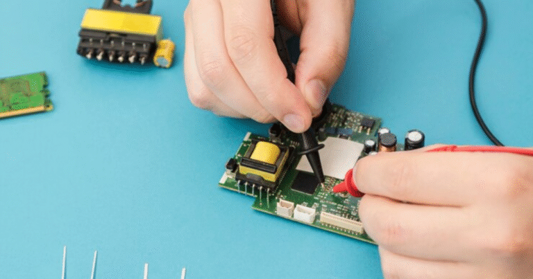
Even the best PCBs require maintenance over time. Repairs involve diagnosing issues like broken traces or faulty components, often using multimeters or oscilloscopes. Damaged components can be replaced, and traces may be reworked with solder or conductive ink. Regular maintenance, such as cleaning to remove dust or corrosion, extends the board’s lifespan and reduces downtime in critical applications.
A well-designed PCB layout offers numerous benefits that enhance device performance and production efficiency.
Thoughtful layouts ensure PCBs withstand mechanical stress, temperature fluctuations, and environmental factors, reducing the risk of failure.
Strategic component placement and thermal vias keep temperatures in check, protecting components from overheating and extending device life.
Optimized trace routing minimizes crosstalk, EMI, and signal loss, ensuring high-speed circuits perform reliably.
Layout design tools catch errors before manufacturing, saving time and costs compared to post-production fixes.
Advanced layouts support cutting-edge technologies like IoT, 5G, and wearable devices, enabling compact and powerful designs.
Designing PCB layouts is not without challenges, especially as electronics become smaller and more complex.
Shrinking devices require fitting intricate circuits into tiny spaces, complicating trace routing and component placement.
High-frequency designs demand precise impedance control and noise reduction, requiring advanced materials and routing techniques.
Modern PCBs rely on sophisticated tools for imaging, drilling, and testing, which can be costly and require skilled operators.
Complex layouts, such as multi-layer or flexible designs, increase production costs, particularly for low-volume runs.
The future of PCB layout is bright, with innovations poised to transform the field. Artificial intelligence (AI) is streamlining design by optimizing layouts and predicting performance issues. Flexible and biodegradable substrates are enabling eco-friendly and wearable electronics. 3D-printed PCBs offer rapid prototyping and customization, while high-speed designs for 5G and beyond push the limits of signal integrity. As these trends evolve, PCB layouts will continue to drive technological progress.
PCB layout is the backbone of electronic design, blending electrical functionality, mechanical precision, and manufacturing efficiency into a single blueprint. By mastering material selection, design considerations, and manufacturing processes, engineers create PCBs that power the devices shaping our world. As technology advances, the role of PCB layout will only grow, enabling innovations that redefine what’s possible.
At Megabyte Circuit, we specialize in crafting high-quality PCB layouts tailored to your needs. Whether you’re a startup or an established industry player, our expertise ensures your designs come to life with precision and reliability. Contact us today to start your next PCB project!
C/10, Yogeshwar Estate, B/H Madhuram Estate, Nr. Vishala Estate, Sardar Patel Ring Rd, Odhav, Ahmedabad, Gujarat, Ahmedabad - 382430, Gujarat (India)
Copyright © 2025. Megabytes Circuit Systems All rights reserved.
Powered by FrogMEE Tech