Ahmedabad - 382430, Gujarat (India)
Custom PCB manufacturing in India has emerged as a critical capability for innovators and businesses seeking tailored electronic solutions. Moving a product from an initial concept to a market-ready device requires a seamless journey from prototyping to full-scale production. This involves not only precision PCB fabrication in India but also a deep understanding of design, material selection, and assembly processes.
Whether you’re looking to develop a single board for testing or require thousands for commercial release, understanding the robust ecosystem for custom PCB India offers is essential. Megabytes Circuit Systems provides comprehensive services to navigate this entire process efficiently, ensuring your designs transform into reliable physical products.
The landscape of electronics manufacturing in India has undergone a significant transformation, with custom PCB manufacturing capabilities expanding rapidly. Historically, many companies relied on international suppliers for specialized PCB needs. However, advancements in technology, skilled labor availability, and supportive government policies have fostered a robust domestic industry. Today, India boasts numerous facilities capable of producing high-quality, complex custom PCBs, catering to diverse sectors such as automotive, medical devices, telecommunications, and consumer electronics.
This growth signifies a maturity in PCB manufacturing in India, enabling local businesses and international clients to leverage efficient production cycles, competitive pricing, and reduced lead times. The ability to source custom PCB India locally simplifies logistics, reduces supply chain risks, and facilitates quicker iteration cycles for product development. This localized expertise covers a broad spectrum of board types, from simple Single Layer PCB designs to intricate Multilayer PCB constructions, ensuring that complex project requirements can be met domestically.
The journey of custom PCB manufacturing in India begins long before any physical board is produced. It starts with a well-defined concept and meticulous design work, culminating in a functional prototype.
Every custom PCB project necessitates a precise design. This involves translating an electrical schematic into a physical layout, considering component placement, signal routing, power distribution, and thermal management. A professional PCB design service is crucial at this stage to ensure optimal performance, manufacturability, and reliability. Designers meticulously create Gerber files and other necessary fabrication data, which serve as the blueprint for manufacturing. Additionally, comprehensive PCB developing services encompass not just layout but also engineering support, DFM analysis, and validation, ensuring the design is ready for the next stages.
Choosing the right materials is fundamental to the performance and cost of a custom PCB India. The selection depends on the application’s requirements, such as operating temperature, frequency, power handling, and mechanical stress. Common materials include various grades of FR-4, but specialized laminates may be required for high-frequency or high-power applications. The number of layers is also a critical specification. While simple applications might suffice with a Single Layer PCB, more complex designs often require a Double Layer PCB or even a Multilayer PCB to accommodate dense circuitry and improve signal integrity. This choice directly impacts complexity, cost, and overall board performance.
Once the design is finalized and materials are specified, the next step in custom PCB manufacturing in India is prototyping. This phase involves producing a small batch of boards to validate the design’s functionality, test its performance, and identify any potential issues before mass production. Prototyping is invaluable for debugging, optimizing component placement, and verifying signal integrity.
It provides a tangible opportunity to refine the design and avoid costly errors in larger production runs. Many companies offering PCB manufacturing in India specialize in rapid prototyping services, allowing for quick turnaround times essential for agile product development. This stage is where “PCB order online India” becomes relevant, as many prototyping services facilitate streamlined online submission of design files and order placement for custom boards.
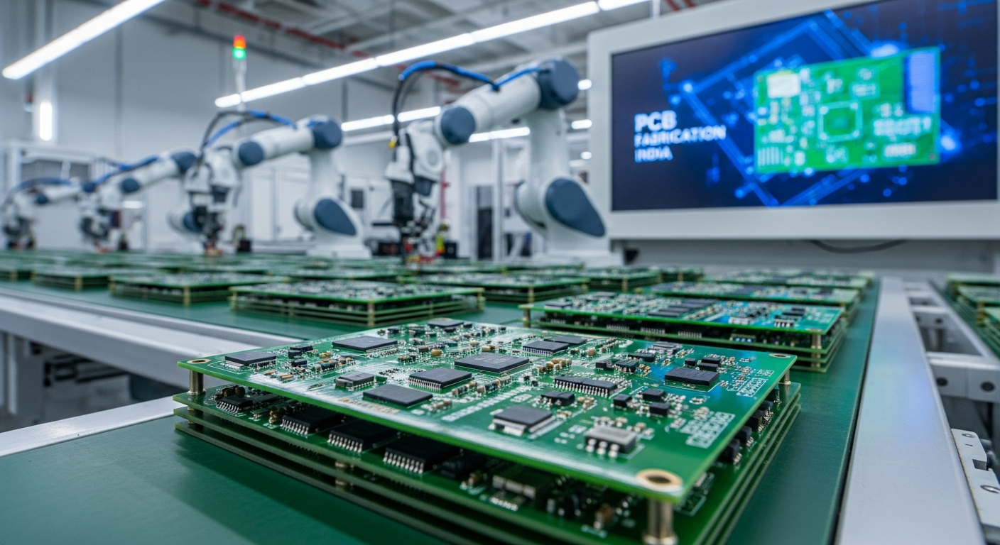
The actual PCB fabrication in India involves a series of intricate steps that transform design data into a physical circuit board. This process requires specialized equipment, skilled technicians, and rigorous quality control.
Before physical production begins, the design files undergo a crucial front-end engineering review. This involves checking the design for manufacturability (DFM) against the specific capabilities and tolerances of the chosen PCB manufacturing in India facility. Engineers analyze Gerber data, drill files, and other specifications to identify any potential issues that could lead to manufacturing defects or increased costs.
This stage ensures that the design is robust and can be fabricated efficiently. It’s also where the production panelization is determined, optimizing the arrangement of multiple boards on a single manufacturing panel to maximize material usage and minimize waste.
The physical custom PCB manufacturing process involves several key stages:
Each of these steps is executed with precision in facilities providing advanced PCB manufacturing service to ensure the integrity and functionality of the final custom PCB.
Throughout the PCB fabrication in India process, rigorous quality control measures are implemented. This includes automated optical inspection (AOI) to check for defects in copper patterns, electrical testing (e.g., flying probe or bed-of-nails) to verify circuit continuity and isolation, and dimensional checks. Final visual inspection ensures that the boards meet all cosmetic and specification requirements. This comprehensive testing is vital to ensure that every custom PCB India produces meets the highest standards of reliability and performance.
Transitioning from a successful prototype to full-scale production is a critical phase in custom PCB manufacturing in India, requiring careful planning and execution.
The insights gained from prototyping are fed back into the design to optimize it for mass production. This involves a more intensive DFM review, focusing on aspects that affect cost, yield, and assembly efficiency at scale. Minor adjustments to trace widths, spacing, via sizes, and panelization can significantly reduce manufacturing costs and improve production yields. This iterative process is essential for achieving cost-effective custom PCB manufacturing in India without compromising quality. Utilizing tools like a PCB Calculator can help estimate costs for various production volumes and design choices, providing valuable data for optimization.
Once the bare PCBs are fabricated, they move to the assembly stage. This is where electronic components are mounted onto the board, creating a functional Printed Circuit Board Assembly (PCBA). Modern PCB Assembly service facilities in India use automated pick-and-place machines for surface mount technology (SMT) components and skilled technicians for through-hole components. After assembly, the boards undergo further testing, including Automated Optical Inspection (AOI), X-ray inspection (for BGA components), In-Circuit Testing (ICT), and functional testing, to ensure that all components are correctly placed and soldered, and the entire assembly functions as intended.
Efficient supply chain management is paramount for successful high-volume custom PCB manufacturing in India. This includes timely procurement of components, coordination with the PCB fabricator and assembler, and managing shipping and delivery. For businesses looking to “order PCB online India” or engage in “PCB online India” transactions, a reliable partner will offer streamlined processes for managing these logistical complexities, ensuring components and boards arrive on schedule and within budget. Effective logistics are key to maintaining production timelines and meeting market demands.
Selecting the right partner for custom PCB manufacturing in India is paramount for project success, impacting everything from product quality to time-to-market and cost.
When choosing a custom PCB India manufacturer, several factors should be meticulously evaluated:
Cost-Effectiveness: While not the sole factor, competitive pricing combined with high quality is always desirable. Services that allow you to “order PCB online India” with transparent pricing, often aided by an integrated PCB Calculator, can simplify the process.
At Megabytes Circuit Systems, we understand the intricate journey of custom PCB manufacturing in India, from a nascent idea to a finished product ready for market. We pride ourselves on offering end-to-end solutions that encompass every stage of your project. Our commitment to excellence in PCB fabrication in India is backed by advanced technology, stringent quality control, and a team of seasoned experts dedicated to bringing your designs to life.
Whether you need a quick prototype or a large-scale production run, our integrated approach covers specialized PCB design service, comprehensive PCB developing services, cutting-edge PCB manufacturing service, and precision PCB Assembly service. We streamline the process for those looking to “order PCB online India,” offering transparency and efficiency. Partner with Megabytes Circuit Systems to transform your innovations into reality with confidence and unparalleled quality.
C/10, Yogeshwar Estate, B/H Madhuram Estate, Nr. Vishala Estate, Sardar Patel Ring Rd, Odhav, Ahmedabad, Gujarat, Ahmedabad - 382430, Gujarat (India)
Copyright © 2025. Megabytes Circuit Systems All rights reserved.
Powered by FrogMEE Tech