Ahmedabad - 382430, Gujarat (India)
The Indian automotive landscape is undergoing a radical shift toward electrification. For hardware engineers and IoT developers, this transition brings a unique set of challenges. Unlike consumer electronics, automotive pcb fabrication for Electric Vehicles (EVs) must handle extreme thermal cycles, high-voltage environments, and constant mechanical vibration. At Megabyte Circuit Systems, we understand that a failure in a Battery Management System (BMS) or a Traction Inverter isn’t just a technical glitch—it’s a safety critical event.
Designing for EVs requires a departure from standard FR4 thinking. You are no longer just routing signals; you are managing power density and ensuring long-term reliability in harsh environments.
Quick Technical Summary: High-voltage PCB design for EVs focuses on maintaining electrical isolation and thermal stability under loads often exceeding 400V–800V. Engineers must prioritize creepage and clearance distances while utilizing heavy copper traces to manage high current densities without catastrophic heat rise.
In a typical Electric Vehicle, the PCB acts as the nervous system and the muscle. From the BMS to the DC-DC converters, these boards must withstand “High-Voltage (HV)” and “Low-Voltage (LV)” signals residing on the same substrate. This necessitates a deep understanding of high voltage pcb design rules.
When you partner with a specialized PCB Manufacturing service, the primary focus is on dielectric breakdown strength. In EV environments, the risk of “tracking” or “arcing” across the board surface is high. Designers must calculate the minimum spacing based on the Comparative Tracking Index (CTI) of the base material. For most EV applications, utilizing a material with a CTI of 600V+ is mandatory to ensure the longevity of the Power Distribution Unit (PDU).
Quick Technical Summary: Heavy copper PCBs (utilizing 3oz to 10oz of copper) are essential for EV inverters and charging systems to conduct high currents and dissipate heat. These boards replace traditional busbars, reducing the weight and complexity of the vehicle’s electrical architecture.
For a leading EV pcb manufacturer india, the demand for heavy copper pcb has skyrocketed. Standard PCBs typically use 1oz (35µm) copper. However, EV power stages often require 3oz, 4oz, or even up to 10oz copper to handle the massive current surges during acceleration and fast charging.
The formula for calculating the required cross-sectional area A of a trace for a given current I and temperature rise ΔT is derived from IPC-2221:
I=k⋅ΔT0.44⋅A0.725
Where:
By using thick copper layers, we reduce the DC resistance of the traces, which directly minimizes I2R losses and heat generation.
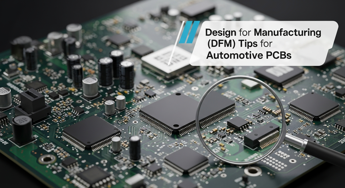
Quick Technical Summary: Automotive DFM focuses on structural integrity, such as teardrop padding to prevent stress fractures and advanced solder mask application to ensure insulation. Engineers should work closely with their fabricator to optimize via-in-pad designs and thermal relief patterns.
When preparing your automotive pcb fabrication files for Megabyte Circuit Systems, consider the following expert DFM tips:
Choosing the right substrate is the difference between a board that lasts 10 years and one that fails in six months.
Feature | Standard FR4 | High-Tg FR4 (IT-180A) | Ceramic Substrate (AlN) | Metal Core PCB (MCPCB) |
Thermal Conductivity | ~0.25 W/mK | ~0.40 W/mK | 150-180 W/mK | 1.0 – 5.0 W/mK |
Glass Transition (Tg) | 130°C – 140°C | 170°C – 180°C | N/A | Variable |
Dielectric Strength | Good | Excellent | Superior | Moderate |
Typical EV Use Case | Infotainment | BMS / ECUs | High-Power Inverters | LED Headlights |
Cost Profile | Low | Medium | High | Medium-High |
For most Multilayer PCB projects in the EV sector, we recommend High-Tg FR4 as the baseline to ensure the board remains dimensionally stable during the high-heat cycles of automotive operation.
Quick Technical Summary: Automotive PCBs must meet IPC-6012DA (Automotive Addendum), which mandates stricter criteria for copper plating thickness and hole wall integrity. Megabyte Circuit Systems employs 100% E-Testing and Flying Probe tests to ensure zero-defect shipments for EV clients.
Reliability is non-negotiable in the automotive world. While consumer electronics often follow IPC Class 2 standards, automotive pcb fabrication usually demands IPC Class 3 or the specific IPC-6012DA automotive addendum. These standards dictate:
At Megabyte, we utilize Flying Probe Testing for prototypes and high-speed Automatic Optical Inspection (AOI) for production runs. This ensures that every Single Layer PCB or complex multilayer stack-up we deliver is ready for the rigors of the road.
Quick Technical Summary: To optimize costs without sacrificing quality, engineers should standardize panel utilization and avoid exotic materials unless thermally necessary. Utilizing a local partner like Megabyte Circuit Systems reduces logistics costs and import duties associated with foreign sourcing.
Managing the “BOM cost” is critical for Indian EV startups. Here is how you can save:
Tooling: For initial prototypes, use our PCB Calculator to compare the cost of different surface finishes (HASL vs. ENIG). While ENIG is better for fine-pitch components, HASL is often more cost-effective for power-heavy boards.
The biggest challenge is managing “Creepage” (distance over the surface) and “Clearance” (distance through the air). For 800V EV systems, these distances must be strictly maintained to prevent catastrophic electrical arcing.
EVs deal with high currents (often 200A or more). Heavy copper allows the PCB to carry this current without overheating, effectively acting as a compact, integrated busbar.
Standard FR4 is fine for low-power control logic. However, for traction inverters and fast-charging modules, High-Tg FR4 or Ceramic substrates are preferred due to their superior thermal performance.
Look for manufacturers who are familiar with IATF 16949 quality management systems and IPC-6012DA automotive standards.
Vibration can cause solder joint fatigue. Designers mitigate this by using smaller components, adding mechanical support, and utilizing “Teardrops” on all pad-to-trace junctions.
The transition to Electric Vehicles is a high-stakes engineering challenge. Success depends on the reliability of your printed circuit boards. Whether you are developing a next-gen two-wheeler BMS or a heavy-duty commercial vehicle inverter, Megabyte Circuit Systems has the technical expertise and manufacturing capability to bring your design to life.
Ready to take your EV project to the next level?
Megabyte Circuit Systems: Powering the Future of Indian Mobility.
C/10, Yogeshwar Estate, B/H Madhuram Estate, Nr. Vishala Estate, Sardar Patel Ring Rd, Odhav, Ahmedabad, Gujarat, Ahmedabad - 382430, Gujarat (India)
Copyright © 2025. Megabytes Circuit Systems All rights reserved.
Powered by FrogMEE Tech