Ahmedabad - 382430, Gujarat (India)
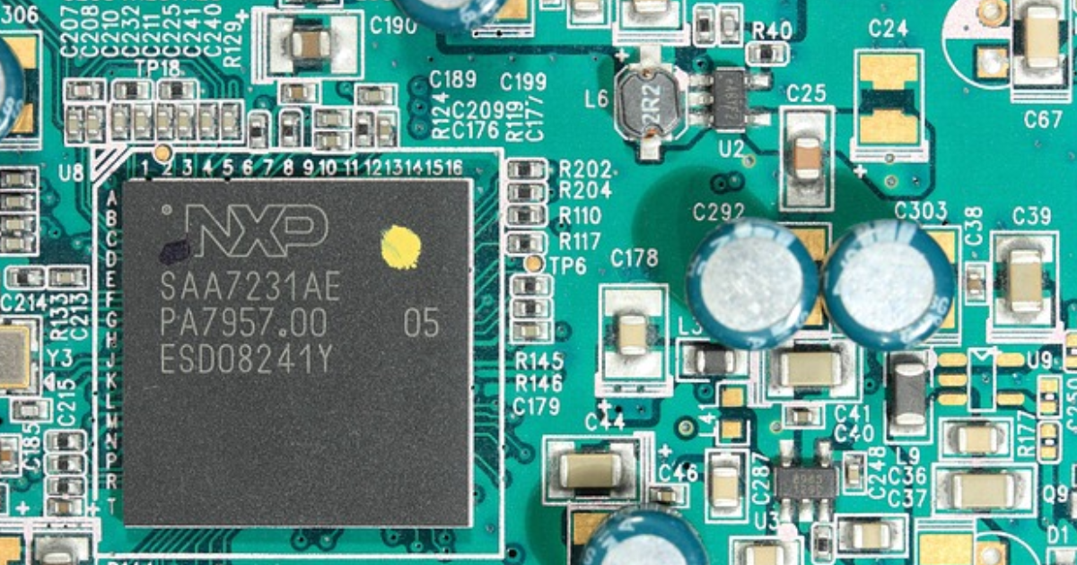
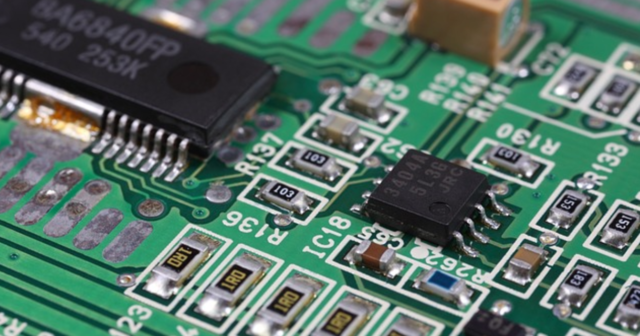
In the rapidly evolving world of electronics, multi-layer boards (also known as multilayer PCBs) have become the backbone of high-performance devices. Unlike single-layer or double-sided printed circuit boards, multilayer PCBs consist of three or more conductive layers separated by insulating materials. These boards are designed to handle complex circuits, offering superior functionality, reliability, and compactness. As industries like aerospace, medical, and telecommunications push the boundaries of technology, multilayer PCBs have emerged as the preferred choice for meeting their demanding requirements.
This blog explores the applications of multilayer PCBs in high-tech industries, their key benefits, and why they are essential for modern electronics. Whether you’re an engineer, a product developer, or a business looking to innovate, understanding the power of multilayer PCBs can help you make informed decisions for your next project. Ready to optimize your circuit design? Contact us for expert PCB fabrication services.
A multilayer PCB is a printed circuit board with multiple layers of copper traces, typically ranging from 4 to 12 layers or more, stacked and bonded together. These layers are interconnected using vias (small conductive holes) to route signals and power efficiently. The complexity of multilayer PCBs allows them to support high-density circuits, making them ideal for advanced applications where space, performance, and reliability are critical.
Unlike single-layer PCBs, which are limited to simple electronics like calculators, or double-sided PCBs used in basic consumer devices, multilayer PCBs excel in scenarios requiring intricate designs, high-speed signals, and robust power management. Their ability to pack more functionality into a smaller footprint has made them indispensable in high-tech industries.
Multilayer PCBs are at the heart of cutting-edge technologies across various sectors. Below, we explore their key applications in aerospace, medical, and telecommunications, with real-world examples to illustrate their impact.
The aerospace sector demands electronics that are lightweight, reliable, and capable of operating in extreme conditions. Multilayer PCBs meet these needs by enabling compact, high-performance circuits for applications such as:
Why Multilayer PCBs? Their ability to handle high-speed signals and reduce electromagnetic interference (EMI) ensures reliable performance in mission-critical aerospace applications.
In the medical field, precision and reliability are non-negotiable. Multilayer PCBs power life-saving devices by supporting complex circuitry in compact forms. Key applications include:
Why Multilayer PCBs? Their high density allows for miniaturization, while their reliability ensures consistent performance in critical medical applications.
The telecommunications sector drives connectivity through devices that require high-speed data transfer and robust signal integrity. Multilayer PCBs are critical in:
Why Multilayer PCBs? They support high-speed signal transmission and reduce signal loss, making them ideal for the demands of modern telecommunications.
A PCB Calculator is an intuitive tool that automates cost estimation, eliminating the need for manual calculations or specialized software. Here’s how it functions at Megabytes Circuit Systems:
The widespread adoption of multilayer PCBs in high-tech industries is driven by their unique advantages. Below are the key benefits that make them the go-to choice for complex electronics.
Multilayer PCBs allow designers to stack multiple layers of circuitry, reducing the board’s footprint. This is critical for applications like smartphones and medical wearables, where space is limited. By integrating more functionality into a smaller area, multilayer PCBs enable sleek, portable devices without sacrificing performance.
High-speed applications, such as 5G networks and avionics, require minimal signal loss and interference. Multilayer PCBs use dedicated ground and power planes to reduce EMI and crosstalk, ensuring clean signal transmission. This is especially important in telecommunications and aerospace, where data accuracy is paramount.
The layered structure of multilayer PCBs provides better thermal management and mechanical stability. By distributing heat and stress across multiple layers, these boards are less prone to failure, making them ideal for harsh environments like space or medical operating rooms.
With multiple layers, designers can separate power, ground, and signal planes, optimizing the board for specific functions. This flexibility allows multilayer PCBs to support complex circuits, such as those in IoT devices or advanced medical equipment, without compromising performance.
While multilayer PCBs may have higher upfront costs than single-layer boards, their ability to integrate multiple functions into one board reduces the need for additional components and connectors. This makes them cost-effective for high-tech applications where performance outweighs initial investment.
Despite their advantages, multilayer PCBs come with challenges. Manufacturing is more complex, requiring advanced equipment and skilled technicians. Design errors, such as improper via placement, can lead to signal issues or board failure. Additionally, testing and debugging multilayer PCBs can be time-consuming due to their layered structure.
Solutions:
To illustrate the impact of multilayer PCBs, consider these examples:
These examples highlight how multilayer PCBs drive innovation across industries, enabling smaller, smarter, and more reliable devices.
Headquartered in Ahmedabad, Gujarat, Megabytes Circuit Systems is a trusted PCB manufacturer in India, recognized for quality and innovation. Our ISO-certified facility produces high-performance boards with rigorous testing for functionality, durability, and compliance. Key advantages include:
Whether you’re managing circuit board expenses or seeking a custom solution, our team is dedicated to your project’s success.
To leverage the benefits of multilayer PCBs, consider these best practices:
At [Your Company Name], we specialize in multilayer PCB production tailored to high-tech industries. Our state-of-the-art facilities and experienced team ensure high-quality boards that meet your specifications. Whether you’re developing aerospace avionics, medical devices, or 5G infrastructure, we’ve got you covered. Contact us now to start your project.
Multi-layer boards are revolutionizing high-tech industries by enabling compact, reliable, and high-performance electronics. From aerospace avionics to medical imaging and 5G telecommunications, multilayer PCBs are the foundation of modern innovation. Their benefits compact design, enhanced signal integrity, and greater reliability make them the preferred choice for complex circuits.
As technology continues to advance, the demand for multilayer PCBs will only grow. By understanding their applications and advantages, you can make informed decisions to optimize your projects. Ready to bring your ideas to life? Request a quote for multilayer PCB fabrication and partner with us to power your next innovation.
C/10, Yogeshwar Estate, B/H Madhuram Estate, Nr. Vishala Estate, Sardar Patel Ring Rd, Odhav, Ahmedabad, Gujarat, Ahmedabad - 382430, Gujarat (India)
Copyright © 2025. Megabytes Circuit Systems All rights reserved.
Powered by FrogMEE Tech