Ahmedabad - 382430, Gujarat (India)
If you’re designing a new IoT device, industrial controller, or compact consumer gadget in India, one question often comes up during the layout stage: Should I go with a standard multilayer PCB or step up to an HDI PCB?
Many hardware engineers and procurement teams I’ve worked with over the years face this exact dilemma. A standard multilayer board feels familiar and budget-friendly, but as components get finer (think 0.4mm or 0.3mm pitch BGAs, high-speed interfaces like PCIe or DDR), space constraints and signal integrity issues push them toward High-Density Interconnect (HDI) technology.
In this guide, I’ll break it down clearly from construction differences to real-world performance, cost implications in the Indian manufacturing context, and practical DFM advice. By the end, you’ll know exactly which one your project needs, and how to optimize your design for reliable fabrication.
Quick Technical Summary
Standard multilayer PCBs use through-hole vias and conventional lamination for 4–16+ layers. HDI PCBs employ microvias (≤150µm), blind/buried vias, and sequential build-up for higher routing density in a smaller footprint. Choose multilayer for cost-sensitive, moderate-density designs; go HDI when you need miniaturization, finer traces, or superior high-speed performance.
A multilayer PCB consists of three or more copper layers laminated together with prepreg and core materials, typically FR4. Connections between layers are made primarily with plated through-hole (PTH) vias that go all the way through the board.
These boards are the workhorse of electronics manufacturing. You can have 4-layer, 6-layer, 8-layer, or even 12–16 layer stack-ups depending on routing complexity, power distribution, and grounding needs.
In my 20+ years at Megabyte Circuit Systems in Ahmedabad, I’ve seen multilayer PCBs handle everything from simple industrial automation boards to moderately complex medical and automotive controllers. They offer good impedance control, solid thermal management with proper plane layers, and are straightforward to fabricate with high yield.
Common features:
If your design fits comfortably in a standard size with these parameters, a multilayer board often gives the best balance of performance and cost.
HDI (High-Density Interconnect) PCBs take multilayer technology further. They achieve significantly higher wiring density per unit area by using microvias (laser-drilled holes typically 50–150µm in diameter), blind vias, buried vias, and sequential lamination processes.
Instead of drilling one big through-hole that wastes space on every layer, HDI allows connections only where needed between adjacent layers or specific build-up layers. This frees up routing channels and lets you pack more components into a smaller board.
HDI stack-ups are often described as 1+N+1, 2+N+2, or even Any-Layer HDI (ELIC). Microvias can be stacked (aligned vertically for maximum density) or staggered (offset for better reliability).
HDI shines in applications demanding miniaturization and high performance:
Quick Technical Summary
HDI uses laser-drilled microvias with low aspect ratios (≤0.8:1 or 1:1) for reliable plating, enabling trace/space down to 3/3 mil or finer. This results in shorter signal paths, reduced parasitic inductance/capacitance, and better EMI control compared to traditional multilayer boards with longer PTH vias.
Here’s a clear side-by-side comparison that many of my clients find helpful when explaining choices to their teams:
Feature | Standard Multilayer PCB | HDI PCB |
Via Types | Primarily through-hole (PTH) | Microvias, blind, buried vias |
Via Diameter | ≥0.3mm (12 mil) | 0.05–0.15mm (2–6 mil) |
Trace/Space | 4–6 mil typical | 2–4 mil or finer |
Routing Density | Moderate | Very High |
Board Size | Larger for same functionality | Significantly smaller & lighter |
Layer Count Efficiency | Needs more layers for complex routing | Achieves same routing in fewer effective layers |
Signal Integrity | Good for most applications | Superior for high-speed (>5GHz) & fine-pitch BGA |
Manufacturing Complexity | Standard lamination & drilling | Sequential build-up, laser drilling |
Typical Cost | Lower | 20–50%+ higher (depends on stack-up) |
Best For | Industrial controls, power electronics, medium IoT | Compact consumer, 5G, medical, automotive ADAS |
The biggest practical difference? Space and signal path length. In HDI, you can fan out a 0.4mm pitch BGA without needing extra layers or board area, and signals travel shorter distances with fewer stubs improving integrity and reducing crosstalk.
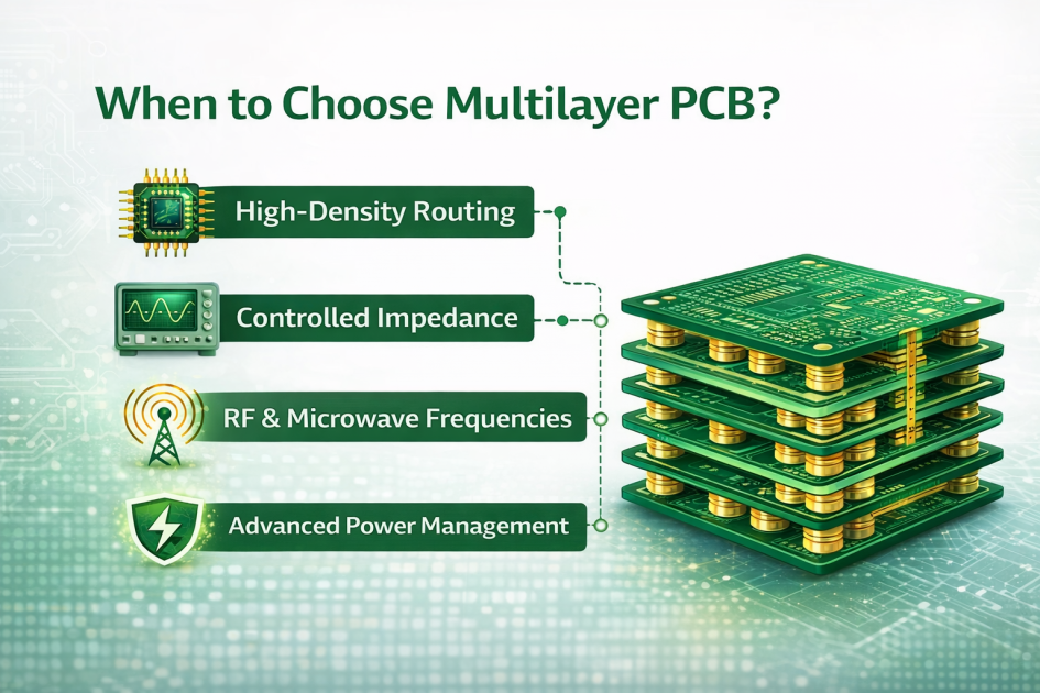
Go with a standard multilayer PCB in these common scenarios:
One thing I always tell startup teams: Don’t over-specify. A well-optimized 6-layer or 8-layer board with good DFM often outperforms a rushed HDI design in both reliability and total project cost.
We frequently recommend starting with multilayer and only moving to HDI when layout tools show you can’t meet size or routing constraints otherwise.
Consider HDI when:
In 2026, with 5G, edge AI, and compact industrial IoT growing fast in India, HDI is becoming the default for many new designs.
However, HDI comes with trade-offs: higher upfront tooling, stricter DFM rules, and potentially longer lead times if your fabricator isn’t experienced.
Quick Technical Summary
Multilayer PCBs suit cost-effective, reliable medium-complexity designs with through vias. HDI excels in miniaturization and high-performance scenarios through microvias and build-up technology, but requires tighter design rules and advanced manufacturing capabilities. Evaluate your component pitch, signal frequency, and target form factor first.
Whether you choose multilayer or HDI, good DFM saves headaches and money. Here’s what I share with every client uploading Gerber files:
For Multilayer PCBs:
For HDI PCBs (Critical):
Common mistake I see: Engineers design in CAD without consulting fabrication limits, then face costly revisions. Always run a DFM check early.
At Megabyte, we review every file and suggest optimizations often reducing layers or improving yield without changing functionality.
Whether multilayer or HDI, quality matters. We follow IPC-A-600 Class 2 or Class 3 standards depending on application, perform flying probe or bed-of-nails electrical testing (E-test), and conduct AOI, X-ray for vias, and cross-section analysis for critical builds.
In India, material consistency (FR4 from trusted suppliers) and process control make a big difference in HDI reliability. Look for fabricators with in-house laser drilling and sequential lamination experience.
Multilayer generally offers lower per-board cost and faster turnaround ideal for prototypes to medium volumes. You can often get competitive pricing with quick-turn options.
HDI costs more due to laser drilling, multiple lamination cycles, and tighter tolerances. However, it can reduce overall system cost by shrinking enclosure size, lowering assembly complexity, or even reducing layer count in some cases.
Tips for best pricing:
Use our PCB Calculator to get instant estimates for both options. Many clients discover that a well-designed multilayer meets 80% of needs at half the premium of HDI.
For complex projects, we also support PCB Design Service and PCB Developing Services to refine your layout for manufacturability.
If you’re exploring basic options first, check our Single Layer PCB, Double Layer PCB, or Multilayer PCB pages.
No. HDI is better when you need higher density or superior high-speed performance in a small form factor. For many industrial and IoT applications in India, a well-designed multilayer PCB delivers excellent reliability at lower cost and faster lead times.
Typically 20–60% higher depending on stack-up complexity, via structure, and volume. However, total product cost (including enclosure and assembly) can sometimes be lower with HDI due to miniaturization.
Yes, often. We help many clients re-layout for HDI to shrink board size or add functionality without increasing layers significantly. Early consultation gives the best results.
Staggered microvias generally offer better reliability than stacked, especially in thermal cycling environments common in Indian industrial applications. Stacked vias save space but need careful filling and plating.
Yes. We fabricate standard multilayer up to 16+ layers and support HDI with microvias and advanced build-ups. Our Ahmedabad facility handles quick-turn prototypes as well as production volumes.
Start with component footprint analysis and routing estimates in your CAD tool. If you struggle with fan-out or hit size limits, evaluate HDI. Share your schematic and preliminary layout with us we’ll give honest feedback on the best option.
Choosing between multilayer PCB and HDI PCB ultimately comes down to your project’s specific needs size, performance, budget, and timeline.
At Megabyte Circuit Systems, based in Ahmedabad, Gujarat, India, we’ve guided hundreds of Indian hardware engineers and startups through exactly this decision. Our team combines deep fabrication expertise with practical design-for-manufacturing advice to deliver reliable boards on time.
Upload your Gerber files today, use the PCB Calculator for instant pricing, or simply request a quote. Whether you need standard multilayer or advanced HDI, we’ll help you get it right the first time.
Have questions about your specific design? Drop us a message I’m always happy to discuss technical details and find the most practical solution for your team.
Let’s build something reliable together.
– Harshil Patel, Senior Consultant, Megabyte Circuit Systems
C/10, Yogeshwar Estate, B/H Madhuram Estate, Nr. Vishala Estate, Sardar Patel Ring Rd, Odhav, Ahmedabad, Gujarat, Ahmedabad - 382430, Gujarat (India)
Copyright © 2025. Megabytes Circuit Systems All rights reserved.
Powered by FrogMEE Tech