Ahmedabad - 382430, Gujarat (India)
Bhopal is steadily building its presence in the electronics and industrial sectors, with growing activity in automation, embedded systems, renewable energy, and startup innovation. From local manufacturers and OEMs to R&D teams and engineering students, more and more projects now depend on reliable, production-ready PCB layouts instead of experimental, trial-and-error boards.
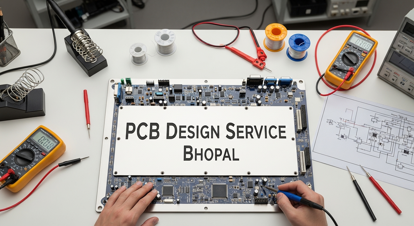
That’s where Megabytes Circuit Systems comes in. Our PCB Design Service in Bhopal helps you convert concepts and schematics into stable, cost-effective, and manufacturer-ready PCB designs. We focus on designs that are not only technically sound on-screen, but also practical to fabricate, assemble, test, and scale. Whether you are developing a small IoT module, an industrial control board, or a complex multilayer product, we support you at every step from design rules to final Gerber files.
Bhopal’s ecosystem includes industrial estates, MSMEs, engineering institutes, and a rising startup culture. Many of these teams work on automation, consumer electronics, EV support hardware, and IoT devices. The common challenge? Turning a working prototype on a breadboard or development kit into a professional PCB that survives real-world use.
Without experienced PCB design, teams often run into:
By choosing a professional PCB Design Service in Bhopal, you can avoid these pitfalls. Megabytes Circuit Systems brings structured design practices, clear documentation, and manufacturability-focused thinking so that your boards are ready for local and national PCB fabricators and assemblers.
At Megabytes Circuit Systems, we treat each PCB as a small engineering project not just a drawing task. When you engage our PCB Design Service in Bhopal, we start by understanding your application, target quantities, expected environment, and budget. This helps us make smart decisions early: layer count, track widths, creepage distances, component footprints, and test options.
Key advantages of working with us include:
For more technical details about our broader capabilities, you can also explore our dedicated PCB Design service and PCB developing services.
Our goal is to act like an extended PCB design team for Bhopal-based businesses, startups, and institutions, someone you can rely on project after project.
A clear, consistent process is essential to get predictable results. Here’s how we typically handle PCB design projects for Bhopal clients:
This process helps ensure that when your PCB reaches the manufacturer, it’s ready for smooth, trouble-free fabrication.
Bhopal’s hardware projects range from student innovations to industrial-grade systems. Our PCB design services are intentionally broad, so we can support you at every stage and complexity level.
Under our PCB Design Service in Bhopal, we design:
When you’re planning your product stack, you can also refer to our product-focused pages for:
We align design rules with common capabilities of Indian PCB manufacturers to keep your boards practical, affordable, and scalable.
Bhopal’s industrial and academic landscape is diverse, and so are the applications that need robust PCB layouts. Our PCB Design Service in Bhopal is well-suited for:
Each sector has its own reliability and cost expectations. We tune layout approaches accordingly for example, additional creepage/clearance for higher voltages, or compact footprints and connectors for consumer-facing devices.
It’s tempting to treat PCB design as a quick CAD activity, but the quality of your layout directly affects product reliability, field performance, and even brand reputation. For Bhopal businesses that want to scale, professional PCB design is a strategic investment, not an optional extra.
By using a specialized PCB Design Service in Bhopal, you can:
Well-planned layouts also make it easier to transition to automated assembly lines in the future. If you eventually pair your design with contract assembly, your assembler will appreciate clear markings, test points, and proper spacing starting from good PCB design.
Bhopal is well-placed between major industrial and tech hubs of Central India, with access to skilled engineering talent and improving infrastructure. This makes it a strong location for building niche electronics products industrial, IoT, energy, and more without always shifting operations to metro cities.
Megabytes Circuit Systems supports this ambition by offering remote yet responsive PCB Design Service in Bhopal. We collaborate via email, calls, and shared design reviews, so your team gets specialist PCB support without needing a full in-house layout department. As your product line grows, we can maintain libraries, design standards, and revision control across multiple boards.
Our primary focus here is PCB layout through our PCB Design Service in Bhopal, but many clients prefer a more complete flow. We can coordinate with trusted fabrication and assembly partners and prepare files suitable for smooth handover. For dedicated manufacturing information, you can explore our other service pages on the Megabytes Circuit website.
Yes. If you already have a schematic or an older layout, we can refine, clean up, or completely re-layout the PCB. This often includes footprint correction, improved placement, better routing of critical signals, and updated documentation, while preserving your core circuit intent.
You will receive Gerber files, Drill files, fabrication notes, stack-up details, Pick & Place files, PDFs of each layer, and the original CAD design files (as per mutual agreement). These are accepted by most PCB manufacturers in India and abroad, making it easy to move to prototype or volume production.
We do support fast-track requirements where feasible, depending on complexity and workload. Share your schematics, constraints, and deadlines, and we’ll advise on the most realistic accelerated plan for your PCB Design Service in Bhopal without skipping essential checks that affect reliability.
Absolutely. Not every project needs a complex multilayer design. We regularly design economical boards that map well to single layer PCB and double layer PCB manufacturing, minimizing cost while keeping quality intact.
Whether you’re refining a prototype, launching a new product line, or upgrading an existing controller, Megabytes Circuit Systems is ready to assist with professional PCB Design Service in Bhopal. We combine practical layout experience, manufacturability awareness, and clear communication to make your PCB journey smoother.
Share your schematic, constraints, and expected quantities, and we’ll suggest a design approach that fits your technical needs and budget. From the first concept to fab-ready files, Megabytes Circuit Systems helps ensure your next PCB is not just functional but reliable, repeatable, and ready for the market.
C/10, Yogeshwar Estate, B/H Madhuram Estate, Nr. Vishala Estate, Sardar Patel Ring Rd, Odhav, Ahmedabad, Gujarat, Ahmedabad - 382430, Gujarat (India)
Copyright © 2025. Megabytes Circuit Systems All rights reserved.
Powered by FrogMEE Tech