PCB Developing Services in Noida

PCB Developing Services in Noida

Driving Innovation with Cutting-Edge PCB Developing Services in Noida

Noida, a leading hub for technology and manufacturing in Uttar Pradesh, thrives on innovation and advanced solutions. Megabyte Circuit Systems provides top-tier PCB developing services in Noida, offering comprehensive solutions for industries such as IT hardware, electronics manufacturing, and telecommunications. We specialize in delivering innovative PCB prototyping, design validation, and testing services to ensure your electronic products meet the highest standards of performance and reliability.

Our state-of-the-art facilities and experienced team guarantee precise and efficient PCB developing in Noida, transforming your concepts into market-ready circuit boards. Whether you’re an innovative startup or an established enterprise in Noida, Megabyte Circuit Systems is your trusted partner for all your PCB development needs.

Why Choose Megabyte Circuit Systems for PCB Developing Services in Noida?

In Noida’s competitive and rapidly evolving technology landscape, selecting the right PCB developing partner is crucial for success. Megabyte Circuit Systems stands out as a leading provider of PCB developing services in Noida, offering:
  • End-to-End Development Solutions: We provide a complete suite of services, from initial design and prototyping to rigorous testing and validation, ensuring a seamless and efficient development process.
  • Advanced Prototyping Technologies: We utilize state-of-the-art prototyping techniques, including 3D printing and rapid PCB fabrication, to quickly and accurately create PCB prototypes.
  • Comprehensive Testing and Validation: Our rigorous testing and validation services ensure that your PCBs meet all required performance specifications, industry standards, and regulatory requirements.
  • Customized Development Approaches: From simple single-layer designs to complex multi-layer PCBs, we tailor our development services to meet your project’s unique requirements, whether for IT infrastructure, consumer electronics, or industrial automation.
  • Rapid Turnaround and Delivery: We prioritize efficiency to meet Noida’s demanding development schedules, helping you accelerate your time to market without compromising quality or innovation.
  • Local Expertise and Dedicated Support: With a deep understanding of Noida’s dynamic industrial ecosystem, we align our services with the city’s specific needs, providing relevant and effective development solutions.
By partnering with us, you gain a dedicated ally committed to delivering PCB developing services in Noida that drive innovation and support the growth of your business.

Our Meticulous PCB Developing Process

At Megabyte Circuit Systems, we follow a detailed and systematic process to ensure that every PCB development project is successful and meets your exact requirements. Our comprehensive approach includes:
  • In-Depth Initial Consultation: We collaborate closely with you to gain a thorough understanding of your project goals, technical specifications, and key constraints, ensuring a clear and aligned vision.
  • Expert Schematic Design and Layout: Our experienced engineers create detailed schematics and PCB layouts, optimizing the design for superior performance, enhanced manufacturability, and cost-effectiveness.
  • Precision Prototyping and Fabrication: We create PCB prototypes using advanced techniques and precision fabrication processes to ensure accurate representation and functionality.
  • Rigorous Testing and Analysis: We conduct comprehensive testing and analysis, including signal integrity analysis, thermal analysis, and EMI/EMC testing, to identify and address potential issues early in the process.
  • Iterative Design Improvements: Based on the test results and analysis, we iterate on the design, making necessary changes and optimizations to improve performance, reliability, and manufacturability.
  • Thorough Design Validation and Verification: We perform comprehensive design validation and verification to ensure that the final design meets all required specifications and industry standards, providing confidence in the final product.
  • Complete Documentation and Support: We provide comprehensive documentation, including schematics, layout files, and test reports, and offer ongoing support to help you transition smoothly from development to manufacturing.
This meticulous process positions us as a top provider of innovative and reliable PCB developing services in Noida, delivering solutions optimized for performance, cost-effectiveness, and long-term reliability.

Industries We Empower in Noida Through PCB Innovation

Industries We Empower in Noida Through PCB Innovation
Noida’s diverse and technology-driven economy requires versatile and reliable PCB developing solutions. We cater to a broad spectrum of sectors, ensuring our development processes meet the specific requirements of each industry:
  • Information Technology (IT) Hardware: Advanced PCB development for servers, networking equipment, and high-performance computing devices.
  • Electronics Manufacturing: Innovative PCB development for consumer electronics, industrial controls, and a wide range of electronic components.
  • Telecommunications: Reliable PCB development for communication devices, network infrastructure, and telecom equipment.
  • Industrial Automation: Dependable PCB development for control systems, sensors, and automation technologies used in manufacturing processes.
  • Medical Devices: High-quality PCB development for medical equipment, diagnostic tools, and patient monitoring systems, adhering to strict regulatory standards.
Our broad cross-industry expertise makes us a preferred choice for PCB developing services in Noida, empowering businesses to achieve technological excellence and drive innovation.

Key Advantages of Local PCB Developing Services in Noida

Partnering with a local PCB developing provider like Megabyte Circuit Systems in Noida offers numerous significant advantages:
  • Accelerated Time-to-Market: Benefit from faster iteration cycles and reduced development time, enabling quicker product launches and faster time to market.
  • Improved Collaboration and Communication: Enjoy enhanced collaboration and more effective communication, ensuring your specific requirements are fully understood and met.
  • Cost-Effective Solutions: Reduce development costs and eliminate potential delays associated with long-distance communication and international collaboration.
  • Direct Involvement and Oversight: Maintain direct involvement in the development process, ensuring that your PCBs meet your stringent quality standards.
  • Support for the Local Economy: Partnering with a local provider supports job creation and strengthens the local economy.

Noida: A Premier Hub for PCB Developing Excellence

Noida’s strategic location as a major IT and manufacturing hub in the National Capital Region (NCR), combined with its strong infrastructure and skilled workforce, makes it an ideal center for PCB developing services. The city boasts a thriving ecosystem of electronics manufacturers, technology companies, and research institutions, all driving innovation and technological advancement.

At Megabyte Circuit Systems, we leverage our local presence to provide PCB developing services that are precisely tailored to the needs of Noida’s industries. Our deep understanding of the local market ensures seamless communication, rapid response times, and solutions that are perfectly aligned with Noida’s unique dynamics.

Our Comprehensive PCB Developing Capabilities in Noida

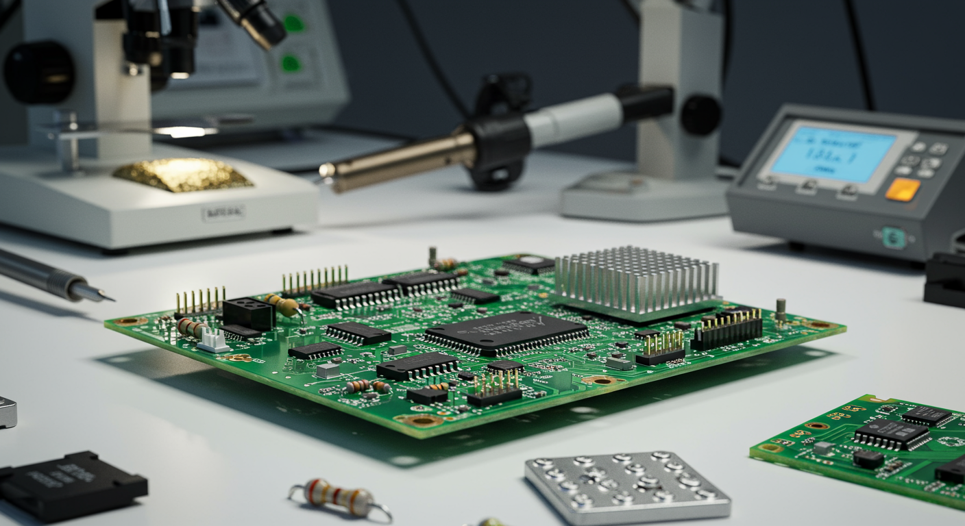
We offer a comprehensive range of PCB developing capabilities in Noida, including:
  • Schematic Design and Layout: Expert design services using industry-leading software and best practices.
  • Prototyping: Rapid prototyping services for quick design validation and functional testing.
  • Signal Integrity Analysis: Advanced simulation and analysis to ensure signal integrity and reliable performance.
  • Thermal Management: Expert thermal analysis and design to prevent overheating and ensure long-term reliability.
  • EMI/EMC Compliance: Design and testing to ensure compliance with electromagnetic interference and compatibility standards.
  • Design for Manufacturability (DFM): Designing PCBs with manufacturing constraints in mind to reduce costs and improve yield.
Our broad and extensive capabilities ensure we can meet the diverse needs of Noida’s industrial sector, delivering precision, reliability, and innovation in every project we undertake.

Frequently Asked Questions (FAQs)

What types of PCB developing services do you offer in Noida?

We provide a comprehensive suite of services, including schematic design, layout, prototyping, signal integrity analysis, thermal management, and EMI/EMC compliance testing.

What is the typical turnaround time for PCB developing projects?

Turnaround times vary depending on the complexity of the project. We offer quick-turn services for urgent projects and strive to meet all deadlines.

What design and simulation tools do you use?

We use industry-leading tools such as Altium Designer, Cadence Allegro, and Ansys HFSS to ensure accurate and reliable results.

Can you help with regulatory compliance for my PCB designs?

Yes, we have extensive experience with regulatory compliance and can help you meet all applicable standards, including RoHS, REACH, and UL.

What file formats do you need for PCB developing services?

We typically require schematics, layout files, and a bill of materials (BOM).

How can I request a quotation for PCB developing services in Noida?

Contact us through our website, Megabyte Circuit Systems, or call us directly to discuss your project requirements. We will promptly provide a customized quote tailored to your specific needs.

Partner with Megabyte Circuit Systems for PCB Developing Excellence in Noida!

Ready to transform your innovative electronic concepts into market-leading products? Megabyte Circuit Systems is your trusted partner for high-quality and reliable PCB developing services in Noida. From initial design to final validation, our dedicated team delivers innovative, efficient, and cutting-edge solutions.

Contact us today to request a quote, explore your project requirements, and discover how we can support your business in Noida’s thriving and dynamic technological ecosystem. Let’s collaborate to engineer the future of electronics!
PCB Developing Services in Noida, PCB Development Noida, PCB Prototyping Noida, PCB Design Noida, PCB Testing Noida, PCB Design and Development Noida, Electronics Design Noida, Circuit Design Noida, Custom PCB Design Noida, PCB Design Services Noida, PCB Design Company Noida, PCB Layout Design Noida, Electronic Engineering Noida, PCB Design Experts Noida, Noida PCB Design Services, Noida Electronics Design, PCB Design Solutions Noida, PCB Design Consultancy Noida, PCB Innovation Noida, PCB Solutions Noida, Electronics Manufacturing Noida