Ahmedabad - 382430, Gujarat (India)
In the high-stakes world of electronic product development, the bridge between a schematic and a functional hardware product is the prototype. For Indian hardware engineers and IoT startups, time-to-market is the ultimate KPI. A delay in receiving a pcb prototype India can mean missing a venture capital milestone or a critical product launch window.
At Megabyte Circuit Systems, we recognize that “fast” isn’t just about shipping speed; it’s about the technical precision of the quick-turn prototyping process. Whether you are developing a Single Layer PCB for a power supply or a complex Multilayer PCB for an AI-on-the-edge device, your prototype serves as the definitive proof of concept. This guide explores the technical parameters, manufacturing standards, and speed-optimized workflows that define the fastest PCB prototype India services in 2026.
Quick Technical Summary: The quick-turn PCB prototyping process compresses traditional 14-day manufacturing cycles into 24–48 hours by utilizing high-speed digital imaging (LDI) and automated CAM validation. This workflow eliminates physical tooling delays, allowing for immediate transition from Gerber files to the etching stage.
When an engineer searches for a pcb prototype India, they are typically looking for an agile response to design iterations. The process at Megabyte begins with an automated CAM (Computer-Aided Manufacturing) review. As soon as you upload your Gerber files (RS-274X or ODB++ formats), our engineers perform a netlist comparison to ensure the physical board will match your electrical intent.
The manufacturing stages for an urgent prototype include:
Quick Technical Summary: DFM optimization for prototypes focuses on eliminating “technical holds” caused by clearance violations or missing drill data. Adhering to standard aspect ratios and providing a complete ODB++ or Gerber X2 package ensures the board moves directly to production without manual intervention.
To guarantee a 24-48 hour turnaround, the design must be “clean.” Our PCB Manufacturing service often encounters delays not due to production capacity, but due to file errors.
When prototyping for high-power IoT devices, calculating the resistance of your traces is vital to avoid overheating. The resistance (R) of a PCB trace is calculated as:
R=w⋅t⋅[1+α(T−Tamb)]ρ⋅L
Where:
By optimizing these variables during the design phase, you ensure that your pcb prototype India performs reliably under real-world thermal loads.
Understanding the differences in manufacturing tolerances helps procurement managers set realistic expectations for their initial builds.
Specification | Standard Prototyping | High-Density Production | Impact on Development |
Turnaround Time | 24 – 48 Hours | 10 – 15 Days | Critical for rapid R&D iterations. |
Min. Trace/Space | 5 mil / 5 mil | 3 mil / 3 mil | Standard prototypes fit most IoT designs. |
Material Base | Standard FR4 (Tg 130-140) | High-Tg FR4, Rogers, Polyimide | Prototypes use versatile, cost-effective FR4. |
Layer Alignment | ± 2 mils | ± 1 mil | Sufficient for standard SMT components. |
Surface Finish | HASL / Lead-Free HASL | ENIG / Hard Gold / ENEPIG | HASL is faster; ENIG is better for BGA. |
If your design requires advanced materials for high-frequency signals, you can check specific material availability using our PCB Calculator.
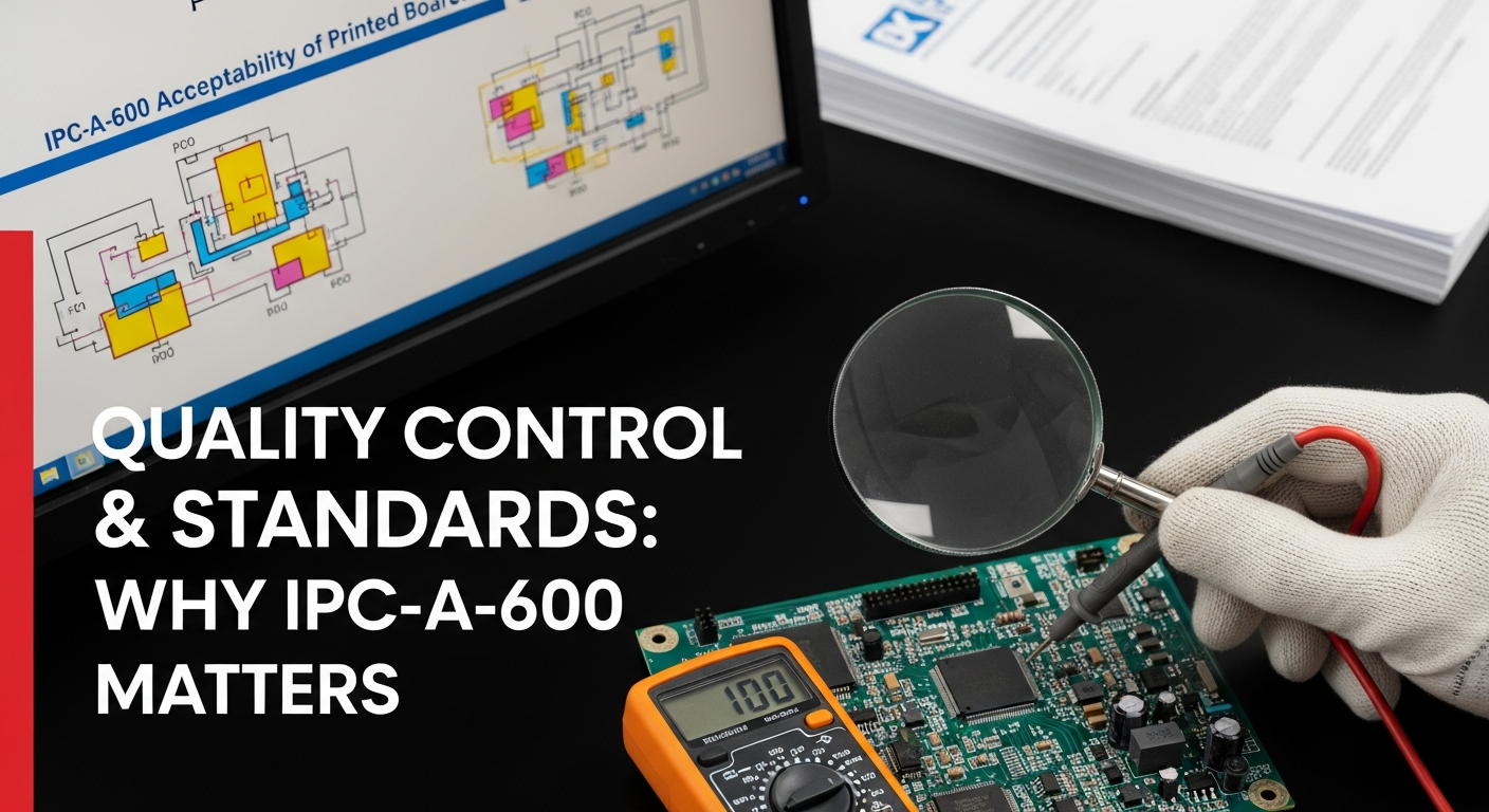
Quick Technical Summary: Quality control for prototypes is governed by the IPC-A-600 standard, which defines the acceptability of printed boards. Megabyte utilizes Flying Probe E-Testing to verify 100% of the netlist, ensuring that even “urgent” boards meet industrial reliability benchmarks.
A fastest PCB prototype India service is useless if the board arrives with “opens” or “shorts.” At Megabyte, we don’t skip quality steps for speed.
By adhering to these rigorous standards, we ensure that your prototype is not just a “dummy board” but a high-fidelity representation of your final product.
Quick Technical Summary: Prototype pricing is primarily driven by the “setup cost” and “turnaround premium” rather than material volume. Optimizing the layer count and utilizing standard FR4 thicknesses are the most effective ways to manage the budget for an RFQ.
While we provide tailored quotes for every project, several technical factors influence the final cost of a pcb prototype India:
To get a precise estimate based on your specific design requirements, please Contact Megabyte Circuit Systems or use our automated tool to input your board dimensions.
Yes. Our facility is optimized for quick-turn multilayer fabrication. As long as the Gerber files pass our initial DFM check, we can manufacture 4-layer and 6-layer boards within a 48-72 hour window.
We prefer RS-274X (Gerber), ODB++, or Gerber X2. Please ensure you include the aperture list and Excellon drill data.
Absolutely. Our PCB Assembly service can handle everything from hand-soldered prototypes to fully automated SMT runs for small batches.
For our standard quick-turn service, we support a minimum trace width and spacing of 4 mils (0.1mm).
No. We understand that R&D requires flexibility. You can order as few as 1 to 5 pieces for your initial testing phase.
In the competitive landscape of Indian electronics, your choice of a fabrication partner determines your speed of innovation. A pcb prototype India should be a seamless experience where speed meets technical excellence. By integrating advanced DFM checks, IPC-compliant manufacturing, and a dedicated 24-48 hour quick-turn line, Megabyte Circuit Systems empowers engineers to fail fast, iterate faster, and succeed sooner.
Take the next step in your design cycle:
C/10, Yogeshwar Estate, B/H Madhuram Estate, Nr. Vishala Estate, Sardar Patel Ring Rd, Odhav, Ahmedabad, Gujarat, Ahmedabad - 382430, Gujarat (India)
Copyright © 2025. Megabytes Circuit Systems All rights reserved.
Powered by FrogMEE Tech