Ahmedabad - 382430, Gujarat (India)
PCB layout design is one of the most critical stages in printed circuit board manufacturing. It determines how efficiently the electronic components will perform once assembled. A well-structured layout can make the difference between a reliable product and one that fails during testing. At Megabyte Circuit System, we specialize in professional PCB layout design services that combine precision, technical expertise, and modern design tools. This blog explains what PCB layout design involves, why it matters, and how our team delivers high-performance designs that meet client and industry standards.
PCB layout design refers to the process of arranging electronic components on a printed circuit board in a way that ensures optimal performance and manufacturability. It’s the step that transforms a circuit schematic into a physical board design ready for fabrication.
In simple terms, PCB layout design decides where each component will sit, how traces will connect them, and how the board will handle power, heat, and signal flow. While schematic design focuses on creating a logical connection between components, layout design ensures these connections are placed correctly on the actual board surface.
Precision is crucial at this stage. Even minor errors in spacing or routing can lead to issues like signal interference, heat buildup, or voltage drops. A well-planned PCB layout improves performance, reduces production costs, and ensures that the final board functions as intended.
A professional PCB layout isn’t just about placing components neatly. It directly affects how your product performs and how cost-effective manufacturing will be. Poor layout design can result in cross-talk, unstable power distribution, and even board failure.
When you work with experienced designers like the team at Megabyte Circuit System, you gain access to a process that balances electrical and mechanical constraints. Every trace, pad, and via is planned with precision to achieve signal integrity, minimize interference, and support heat dissipation.
Professional layout design also ensures that your PCB is compliant with manufacturing standards. This reduces the chances of production errors and rework. For example, optimized component placement shortens trace lengths, reduces noise, and supports automated assembly. It also simplifies debugging and maintenance later.
In one instance, a client’s circuit design faced frequent signal dropouts. After our layout redesign, the noise was reduced by over 60%, and the product passed all functional tests on the first run. That’s the power of expert PCB layout design.
Megabyte Circuit System provides complete PCB layout design solutions for businesses of all sizes, from startups to established manufacturers. Our engineers have years of experience handling complex boards that require both technical precision and manufacturing awareness.
We design a wide range of boards, including:
Our team works with leading design software such as Altium Designer, KiCAD, OrCAD, and Eagle. This ensures that we can handle diverse project requirements and file formats.
Each layout is reviewed through rigorous quality checks to ensure compliance with electrical and mechanical standards. From impedance control to trace optimization, every detail is validated before design release.
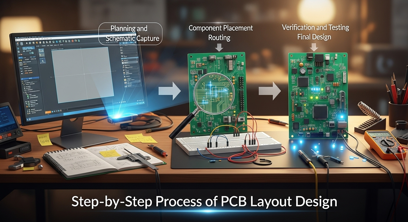
At Megabyte Circuit System, we follow a systematic approach that blends engineering expertise with industry best practices.
This process allows us to deliver PCBs that perform well during testing and mass production. Special attention is given to spacing, thermal balance, and electromagnetic compatibility to ensure the board is both functional and durable.
Our PCB layout design services cater to a wide range of industries. Each sector comes with its own design challenges, and our engineers are trained to handle those specific needs.
Whether it’s a simple Double-layer design or a complex multilayer board, we ensure every project aligns with the performance expectations of the target application.
Choosing Megabyte Circuit System for PCB layout design means working with a team that values precision and client satisfaction.
We offer:
Our goal is to create layouts that are not only functionally strong but also optimized for fabrication, assembly, and long-term reliability.
To stay ahead in PCB design innovation, we apply several advanced techniques during layout creation.
We integrate impedance control and high-speed routing methods for signal stability. Our designs include thermal management strategies and EMI/EMC shielding to minimize interference in sensitive circuits.
Every layout is prepared with Design for Manufacturing (DFM) and Design for Testing (DFT) principles. This means the board is not just optimized for function but also easy to produce and test.
We also use advanced simulation tools to analyze current flow, signal reflection, and thermal distribution before finalizing the design. This proactive approach prevents costly errors later in production.
Megabyte Circuit System has become a trusted name among Indian manufacturers for high-quality PCB layout design. Our clients value our technical expertise, responsive communication, and consistent delivery standards.
Being based in India allows us to provide local support, fast response times, and better cost efficiency. Our collaborative process ensures that clients receive updates at every stage, keeping the design aligned with their product vision.
With our established relationships with PCB manufacturers, we provide a smooth transition from design to fabrication. This reduces delays and ensures the layout is fully optimized for real-world production.
Our growing client base includes companies in sectors like electronics, automotive, and IoT who rely on us for dependable and timely PCB design support.
If you’re looking for professional PCB layout design services in India, Megabyte Circuit System is ready to help. Our experienced engineers deliver accurate, manufacturable, and high-performance designs that support your product goals.
Reach out to our team for a quick consultation or quote. Share your schematic, and we’ll guide you through the complete layout design process from planning to prototype-ready files.
Contact us today to start your next PCB layout project with confidence.
C/10, Yogeshwar Estate, B/H Madhuram Estate, Nr. Vishala Estate, Sardar Patel Ring Rd, Odhav, Ahmedabad, Gujarat, Ahmedabad - 382430, Gujarat (India)
Copyright © 2025. Megabytes Circuit Systems All rights reserved.
Powered by FrogMEE Tech