Ahmedabad - 382430, Gujarat (India)
For startups, hobbyists, and engineers, creating a prototype PCB in India is a critical step in turning innovative ideas into functional products. A prototype printed circuit board (PCB) is a preliminary version of a circuit board used to test designs before mass production. With India emerging as a hub for electronics manufacturing, prototyping has become more accessible and cost-effective. Whether you’re designing a smart device, IoT module, or medical equipment, understanding the prototyping process in India can save time, reduce costs, and ensure quality.
This comprehensive guide walks you through the process of creating your first prototype PCB in India, covering local manufacturers, costs, challenges, and a step-by-step approach. By leveraging India’s growing PCB industry, you can bring your vision to life efficiently. Ready to start your prototyping journey? Contact us for expert PCB fabrication services.
India’s electronics sector is booming, driven by government initiatives like “Make in India” and a skilled workforce. Here’s why PCB board fabrication in India is ideal for prototyping:
For startups and hobbyists, these advantages make India an attractive destination for prototyping innovative electronics.
Follow this detailed process to develop your first prototype PCB in India, from concept to finished board.
Before contacting a manufacturer, clarify your project’s specifications:
Tip: Use a checklist to ensure all requirements are documented. This helps manufacturers provide accurate quotes.
Use PCB design software to create your schematic and layout:
Case Study: A Bangalore-based startup designing an IoT sensor used KiCad to create a 4-layer prototype PCB, reducing design costs by 30% compared to proprietary software.
Choosing the right manufacturer is critical for quality and reliability. Look for:
Top Indian Manufacturers:
Tip: Request quotes from multiple manufacturers to compare pricing and lead times. Get a quote from our trusted PCB fabrication services.
Gerber files are the industry-standard format for PCB manufacturing. They include:
Use your design software to export Gerber files and verify them using a Gerber viewer (e.g., Gerbv). Submit these files to your chosen manufacturer along with a Bill of Materials (BOM) listing all components.
Common Mistake: Incomplete Gerber files can delay production. Double-check that all layers are included.
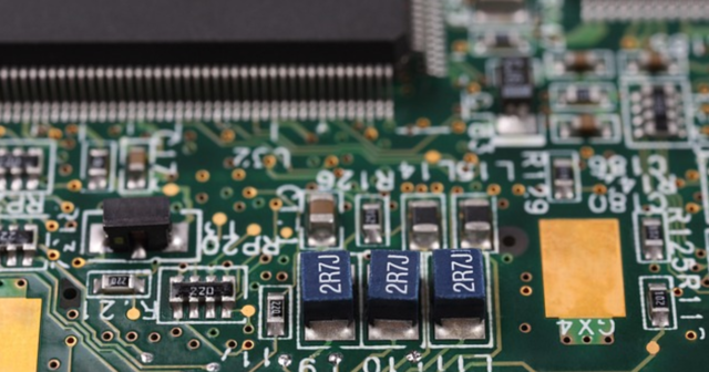
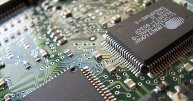
The manufacturer will fabricate your PCB based on the provided files. The process includes:
Lead times for PCB board fabrication in India typically range from 3–10 days for prototypes, depending on complexity.
After fabrication, components are mounted on the board:
Testimonial: “We partnered with a Delhi-based PCB fabricator for our prototype. Their SMT assembly saved us 40% on production time,” says Anil K., a startup founder.
Test your prototype to ensure it meets design expectations:
Tip: Order extra prototype boards to test multiple iterations and avoid delays.
Based on test results, refine your design and order additional prototypes if needed. Once satisfied, transition to small-batch or full-scale production with the same manufacturer to maintain consistency.
The cost of prototype PCB in India depends on several factors:
Example: A 2-layer, 10×10 cm prototype with SMT assembly typically costs $30–$80 in India, compared to $100–$200 in the US.
Tip: Use a PCB cost calculator to estimate expenses and optimize your design for cost savings. Try our PCB cost calculator today.
While India offers many advantages, prototyping can face challenges:
Case Study: A Pune-based hobbyist faced delays due to incomplete Gerber files. By working closely with their manufacturer’s design team, they resolved the issue and received their prototype in 5 days.
At [Your Company Name], we specialize in PCB board fabrication in India, offering quick-turn prototypes tailored to startups and hobbyists. Our ISO-certified facilities and experienced team ensure high-quality boards at competitive prices. Whether you need a single-layer prototype or a complex multilayer design, we’re here to help. Request a quote for your prototype PCB today.
Creating a prototype PCB in India is an exciting opportunity for startups and hobbyists to innovate affordably. By following the step-by-step process defining requirements, designing, selecting a manufacturer, and testing you can develop a high-quality prototype that sets the stage for successful production. India’s cost-effective manufacturing, skilled workforce, and growing infrastructure make it an ideal destination for PCB prototyping.
Overcome challenges like quality variability and supply chain delays by partnering with reputable manufacturers and leveraging tools like PCB design software and cost calculators. Ready to bring your idea to life? Contact us for expert PCB prototyping services and start building your future today.
C/10, Yogeshwar Estate, B/H Madhuram Estate, Nr. Vishala Estate, Sardar Patel Ring Rd, Odhav, Ahmedabad, Gujarat, Ahmedabad - 382430, Gujarat (India)
Copyright © 2025. Megabytes Circuit Systems All rights reserved.
Powered by FrogMEE Tech