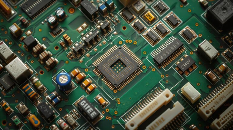
At the heart of every electronic device lies a critical component that ensures seamless functionality: the Printed Circuit Board (PCB). A PCB is a flat, sturdy board crafted from insulating materials such as fiberglass or composite epoxy, with intricate conductive pathways—typically made of copper—etched or printed onto its surface. These pathways serve as the highways for electrical signals, connecting components like resistors, capacitors, integrated circuits (ICs), and more to create a fully operational circuit.
PCBs are ubiquitous, powering everything from everyday gadgets like smartphones, laptops, and smartwatches to sophisticated systems in medical equipment, aerospace technology, and industrial machinery. By replacing cumbersome wiring with a compact and organized structure, PCBs enable manufacturers to build reliable, efficient, and space-saving circuits that drive modern innovation.
This comprehensive guide dives deep into the world of PCBs, covering their structure, types, manufacturing process, and advanced concepts. Whether you’re a hobbyist, engineer, or business owner, you’ll gain a clear understanding of why PCBs are indispensable and how they shape the electronics industry. Here’s what we’ll explore:

A PCB serves as both a physical platform and an electrical roadmap for electronic components. It holds components securely in place while its copper pathways—known as traces—act like wires, enabling the flow of power and signals between them. This organized connectivity ensures that devices function as intended, whether they’re processing data, amplifying signals, or powering displays.
The elegance of a PCB lies in its simplicity and efficiency. By consolidating complex circuitry onto a single board, it eliminates the need for tangled wires and reduces the risk of electrical faults. The result is a compact, durable, and highly reliable solution that can be mass-produced for consumer electronics or customized for specialized applications.
To understand how a PCB functions, let’s break down its essential components:
Together, these elements create a robust and functional board that can support a wide range of electronic applications.
The choice of material is a foundational aspect of PCB layout, as it affects the board’s electrical properties, thermal behavior, and durability. Different materials are selected based on the application’s requirements, such as flexibility, heat dissipation, or high-frequency performance. Below are the most commonly used materials:
Each material brings unique advantages, and selecting the right one ensures the PCB meets the electrical, mechanical, and environmental demands of its intended use.
PCBs are not one-size-fits-all; they come in various forms tailored to specific needs and industries. The choice of PCB type depends on factors like circuit complexity, size constraints, and environmental conditions. Below, we explore the most common types and their applications.
The simplest form of PCB, a single-layer board features one conductive copper layer on a substrate. These boards are cost-effective and ideal for basic electronics, such as calculators, power supplies, or low-cost consumer devices. Their straightforward design makes them easy to manufacture and assemble, but they lack the capacity for complex circuits.
Double-layer PCBs have copper layers on both sides of the substrate, connected by small holes called vias. This design allows for more intricate circuits, making them suitable for applications like automotive dashboards, LED lighting systems, and home appliances. The added flexibility of dual-sided connections supports moderately complex designs without significantly increasing costs.
For high-performance electronics, multi-layer PCBs are the go-to choice. These boards consist of four or more copper layers separated by insulating materials, enabling dense and sophisticated circuitry. They power advanced devices like smartphones, servers, medical imaging systems, and telecommunications equipment. The layered structure enhances signal integrity and supports high-speed data transfer, but it requires precise manufacturing.
Unlike rigid PCBs, flexible PCBs are made from bendable materials like polyimide, allowing them to conform to unique shapes or fit into tight spaces. These boards are essential for wearable technology, foldable smartphones, and aerospace systems where weight and flexibility are critical. Their ability to withstand vibration and bending makes them durable in dynamic environments.
Rigid-flex PCBs combine the best of both worlds: rigid sections for structural support and flexible sections for adaptability. This hybrid design is used in applications like military equipment, medical implants, and advanced robotics, where reliability and compactness are paramount. By reducing the need for connectors and cables, rigid-flex PCBs enhance durability and streamline assembly.
HDI PCBs represent the pinnacle of miniaturization, featuring ultra-fine traces, micro-vias, and high component density. These boards are critical for cutting-edge electronics like 5G devices, IoT sensors, and compact medical devices. Their ability to pack more functionality into smaller spaces drives innovation in industries where size and performance are non-negotiable.
Creating a PCB is a meticulous process that blends engineering precision with advanced technology. Each step is carefully executed to ensure the board meets strict performance and reliability standards. Here’s a detailed look at how PCBs are made.
The journey begins with circuit design, where engineers use specialized software like Altium Designer, KiCad, or Eagle to create a schematic of the circuit. This blueprint outlines how components will connect and function. Once finalized, the schematic is converted into Gerber files—a universal format that guides the manufacturing process by specifying the board’s layout, layers, and features.
The choice of base material is critical, as it affects the PCB’s durability, thermal performance, and electrical properties. FR4 is the most common substrate for rigid PCBs, while polyimide is used for flexible boards and aluminum for heat-dissipating applications. The selected material is cut into precise sizes using automated machinery, preparing it for further processing.
Precision drilling creates holes for component leads and vias, which connect different layers of the PCB. Computer Numerical Control (CNC) machines ensure accuracy, as even minor deviations can disrupt connectivity. Vias are later plated to establish electrical pathways between layers.
To enable inter-layer connections, drilled holes are electroplated with a conductive material, typically copper. This process, known as Plating Through Holes (PTH), ensures robust electrical pathways across the board, especially in multi-layer designs.
The circuit pattern is formed through photolithography, where a photosensitive dry film is applied to the copper layer. The film is exposed to ultraviolet (UV) light through a mask, hardening the areas that will become traces. Unwanted copper is then etched away using chemical solutions, leaving behind the precise conductive pathways.
A protective solder mask is applied to shield the copper traces from environmental damage and prevent unintended solder connections during assembly. Available in various colors (green being the most common), the solder mask enhances the board’s longevity and reliability.
The silkscreen layer adds visual clarity by printing labels, component identifiers, and logos onto the PCB. This step aids technicians during assembly and troubleshooting, ensuring components are placed correctly.
A surface finish is applied to exposed copper areas to enhance solderability and protect against oxidation. Common finishes include:
Each finish is chosen based on the PCB’s intended use and performance requirements.
Quality assurance is critical. Automated Optical Inspection (AOI) scans the board for visual defects, while Flying Probe Testing checks electrical connectivity by probing specific points. These tests identify issues like open circuits or shorts before the board moves to assembly.
The finished PCBs are cut into individual units using CNC routing or V-scoring, a technique that creates grooves for easy separation. The boards are then cleaned, inspected, and packaged for shipment to assembly facilities or customers.

A high-quality PCB is defined by its reliability, performance, and durability. Manufacturers strive to achieve perfection in every aspect of the board, as even minor flaws can lead to device failure. Key characteristics of a superior PCB include:
By adhering to strict design and manufacturing standards, top-tier PCBs deliver consistent performance in demanding environments.
As electronics evolve, so do PCBs, incorporating advanced materials and techniques to meet modern demands. Let’s explore some key concepts driving innovation.
Prepreg, short for pre-impregnated fiberglass, is a critical material in multi-layer PCBs. It consists of fiberglass cloth soaked in an uncured resin, which remains pliable until heated during the lamination process. When pressed and heated, prepreg bonds the core layers of a PCB, providing insulation and structural stability. Its ability to fill gaps and ensure uniform bonding makes it essential for complex, high-layer-count boards.
The solder mask is more than just a colorful coating; it’s a protective polymer layer that safeguards the PCB’s copper traces. By preventing solder bridges, oxidation, and damage from dust or moisture, the solder mask extends the board’s lifespan. While green is the traditional color, manufacturers now offer blue, red, black, and even white solder masks to suit aesthetic or functional needs.
High-Density Interconnect (HDI) PCBs are designed for compact, high-performance electronics. They feature micro-vias (tiny holes less than 150µm in diameter), ultra-fine traces, and densely packed components, enabling smaller, lighter devices without sacrificing functionality. HDI boards are vital for applications like 5G smartphones, IoT devices, and medical wearables.
Taking it a step further, Ultra-High Density Interconnect (UHDI) PCBs push the boundaries with traces finer than 15µm and even smaller vias. UHDI technology is paving the way for next-generation electronics, where miniaturization and speed are critical.
The PCB industry is constantly evolving to keep pace with technological advancements. Some exciting trends shaping the future include:
These innovations highlight the dynamic nature of PCB technology, ensuring it remains at the forefront of electronic innovation.
Printed Circuit Boards are the unsung heroes of the electronics world, enabling everything from pocket-sized gadgets to mission-critical systems. Their ability to combine compactness, reliability, and versatility has made them indispensable across industries. As technology advances, PCBs continue to evolve, incorporating cutting-edge materials, designs, and manufacturing techniques to meet the demands of tomorrow’s devices.
At Megabyte Circuit, we’re passionate about bringing your ideas to life with high-quality prototype PCBs in Ahmedabad. Whether you’re a startup developing a groundbreaking product or an engineer refining a complex design, our precision manufacturing and expert guidance ensure your PCBs meet the highest standards.
Ready to start your PCB project? Contact us today to explore custom solutions tailored to your needs!
C/10, Yogeshwar Estate, B/H Madhuram Estate, Nr. Vishala Estate, Sardar Patel Ring Rd, Odhav, Ahmedabad, Gujarat, Ahmedabad - 382430, Gujarat (India)
Copyright © 2025. Megabytes Circuit Systems All rights reserved.
Powered by FrogMEE Tech
