Ahmedabad - 382430, Gujarat (India)

If you are designing a new electronic product and wondering how components actually get mounted onto your PCB, you are in the right place. Understanding the SMT assembly process is essential for making smart design decisions, reducing rework, and keeping your production costs under control.
In this guide, I will walk you through everything you need to know about surface mount technology, from the basic concept to each step in the process line. We will compare SMT with through-hole assembly, cover design for manufacturing tips, discuss quality standards, and share practical cost optimization strategies that work specifically in the Indian manufacturing context. At Megabyte Circuit Systems, our PCB assembly service handles SMT projects ranging from quick-turn prototypes to high volume production runs, and I have drawn on that real-world experience throughout this article.
Here is what we will cover: the core definition, step-by-step process breakdown, SMT vs through-hole comparison, DFM tips, quality control standards, cost optimization, and frequently asked questions.
SMT (Surface Mount Technology) assembly is the process of mounting electronic components directly onto the surface of a printed circuit board using automated machinery, solder paste, and reflow soldering. Unlike older through-hole methods where component leads pass through drilled holes, SMT components (called SMDs, or Surface Mount Devices) sit flat on copper pads on the board’s surface.
This method is the dominant assembly technology in modern electronics manufacturing. It accounts for roughly 90% of all PCBA assembly worldwide. The reason is simple: SMT allows for smaller components, higher component density, faster automated placement, and significantly lower per-unit costs at volume.
SMT components come in standardized package types such as BGA (Ball Grid Array), QFP (Quad Flat Package), 0402, 0201, and even 01005 chip resistors and capacitors. The choice of package directly impacts your design density, assembly yield, and cost.
Quick Technical Summary: SMT assembly mounts components directly onto PCB surface pads using solder paste and reflow soldering. It enables higher density, smaller boards, and faster production compared to through-hole technology, and it is the standard for over 90% of modern electronics manufacturing.
The SMT process follows a precise, repeatable sequence on an automated production line. Each step has specific parameters and tolerances that directly affect the quality of your finished boards. Here is the complete breakdown.
The process begins with solder paste application. A laser-cut stainless steel stencil (typically 0.10mm to 0.15mm thick) is aligned over the bare PCB. Solder paste, a mixture of microscopic tin-silver-copper (SAC305) alloy spheres and flux, is pushed across the stencil using a squeegee blade at controlled pressure (typically 3 to 8 kg) and speed (20 to 80 mm/s).
Proper paste deposition is critical. The industry target is a transfer efficiency of 80% to 100%, with volume consistency within plus or minus 10%. Most defects in SMT can be traced back to poor solder paste printing.
Immediately after printing, a Solder Paste Inspection machine uses 3D laser measurement to verify paste volume, height, area, and position on every single pad. This is not optional on a professional line. SPI catches over 70% of potential defects before a single component is placed.
High-speed pick-and-place machines use vacuum nozzles to pick components from reels, trays, or tubes and place them onto the solder paste with extreme precision. Modern machines achieve placement speeds of 30,000 to 80,000 components per hour with positional accuracy of plus or minus 0.025mm.
For fine-pitch components like 0.4mm pitch BGAs or 0201 passives, we use vision-aligned placement heads that verify each component before setting it down. This step relies heavily on an accurate pick-and-place file (also called a centroid or XY file) exported from your PCB design software.
The populated board passes through a reflow oven with carefully profiled temperature zones. A standard lead-free reflow profile has four stages:
Nitrogen reflow is used for high-reliability boards to reduce oxidation and improve wetting. The entire profile must comply with component manufacturer specifications and IPC J-STD-001 soldering standards.
After reflow, every board goes through AOI (Automated Optical Inspection). The machine photographs each solder joint and component and compares it against the reference design. AOI detects issues like solder bridges, tombstoning, missing components, polarity errors, and insufficient solder.
For BGA and bottom-terminated components where joints are hidden, X-ray inspection is the standard verification method.
Any defects flagged by AOI or X-ray are addressed by trained rework technicians. This may involve hot air rework stations, soldering irons, or BGA reballing equipment. Professional rework follows IPC-A-610 Class 2 or Class 3 acceptance criteria depending on the product application.
Quick Technical Summary: The SMT process follows six key steps: solder paste printing, SPI, pick-and-place, reflow soldering, AOI, and rework. Each step has specific parameters. Solder paste printing quality alone accounts for the majority of potential defects, making SPI a critical checkpoint.
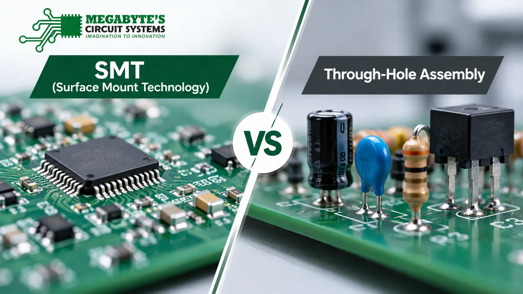
One of the most common questions I get from engineers is whether they should design for SMT, through-hole, or a mix of both. Here is a direct comparison based on real production parameters.
Parameter | SMT Assembly | Through-Hole Assembly |
Component size | As small as 01005 (0.4mm x 0.2mm) | Minimum lead pitch around 2.54mm |
Component density | Very high, both sides of PCB | Lower, typically single side |
Assembly speed | 30,000 to 80,000 CPH | 1,000 to 5,000 insertions per hour |
Mechanical strength | Lower (surface bond only) | Higher (lead through barrel + solder) |
Soldering method | Reflow soldering | Wave soldering or selective soldering |
Typical applications | Consumer electronics, IoT, mobile | Power supplies, connectors, high-vibration environments |
Per-unit cost at volume | Lower | Higher |
Rework difficulty | Moderate to high (BGA rework needs X-ray) | Easier for single components |
When to choose SMT: Use it for compact designs, high density boards, and any product going into volume production. If your multilayer PCB design has hundreds of passives and fine-pitch ICs, SMT is the only practical option.
When to choose through-hole: Use it for components that face mechanical stress, such as large connectors, power terminals, and high-current inductors. Many designs use a mixed approach with SMT for most components and selective through-hole for specific parts.
When to use both: In my 20+ years of experience, roughly 60% of the boards we assemble at Megabyte use a mixed technology approach. This gives you the density advantages of SMT with the mechanical reliability of through-hole where it matters.
Quick Technical Summary: SMT offers smaller components, higher density, and faster assembly at lower cost per unit. Through-hole provides superior mechanical strength. Most real-world designs use a mixed approach, combining SMT for density with selective through-hole for connectors and power components.
Design for Manufacturing is where you save real money and avoid production headaches. One thing I always tell my clients is that 80% of assembly problems originate in the design phase. Here are actionable DFM tips for your SMT project.
Even on a single layer PCB project, following these rules will improve your first-pass yield dramatically.
Quick Technical Summary: Effective DFM for SMT includes proper pad spacing (minimum 0.2mm), standard IPC-7351 footprints, fiducial marks, 5mm board edge clearance, consistent component orientation, and complete file submission. Addressing DFM in the design phase prevents 80% of assembly defects.
At Megabyte Circuit Systems, every SMT assembly job passes through a multi-stage quality control process. We follow IPC-A-610 (Acceptability of Electronic Assemblies) as the primary workmanship standard, with Class 2 as the default and Class 3 for high-reliability applications in defense, medical, and automotive projects.
Key quality checkpoints include:
Soldering processes follow IPC J-STD-001 (Requirements for Soldered Electrical and Electronic Assemblies). All solder paste, flux, and cleaning materials meet IPC J-STD-004 and J-STD-005 specifications.
We maintain solder joint defect rates below 50 DPMO (Defects Per Million Opportunities) on standard production runs. For high-reliability Class 3 work, the target tightens to below 20 DPMO.
Quick Technical Summary: Professional SMT quality control follows IPC-A-610 for workmanship and IPC J-STD-001 for soldering. A robust quality process includes SPI, AOI, X-ray (for BGA), flying probe testing, and visual inspection, targeting defect rates below 50 DPMO.
Getting the best price on your high volume SMT assembly services does not mean cutting corners. It means making smart design and procurement decisions upfront. Here are practical strategies we recommend to our clients.
Standardize your component packages. Using fewer unique package types reduces pick-and-place setup time and nozzle changes. A BOM with 15 unique packages assembles faster and cheaper than one with 40.
Design for panelization. Work with your fabricator to maximize the number of boards per panel. This reduces handling time and improves throughput on the SMT line. Use our PCB calculator to get instant cost estimates based on your board dimensions and panel configuration.
Consolidate your BOM. Wherever possible, use common values across your resistors and capacitors. Going from 50 unique passives to 30 can reduce placement cost by 10% to 15%.
Avoid unnecessarily small packages. Unless your design absolutely requires 0201 or 01005 components, stick with 0402 or 0603 sizes. Smaller packages need slower placement speeds and tighter process controls, both of which increase cost.
Order in production-friendly quantities. SMT has significant setup cost. Per-board cost drops substantially once you cross 100+ units, and the sweet spot for Indian contract manufacturing is typically 500 to 5,000 units for mid-volume runs.
Quick Technical Summary: SMT assembly costs in India can be optimized by standardizing component packages, designing for panelization, consolidating BOM values, avoiding unnecessarily small packages, and ordering in quantities above 100 units. Design-stage decisions have the biggest impact on final assembly cost.
SMT (Surface Mount Technology) refers to the assembly process and method of mounting components. SMD (Surface Mount Device) refers to the components themselves. In other words, SMDs are the parts, and SMT is the process used to assolder them onto the board.
Most professional assemblers, including Megabyte Circuit Systems, offer SMT assembly starting from as few as 5 to 10 prototype boards. Production runs typically start at 100+ units, with significant cost advantages appearing at 500+ units.
Yes. Mixed technology boards are very common. SMT components are placed and reflow soldered first. Through-hole components are then inserted and soldered using wave soldering or selective soldering in a second pass.
You need four essential files: Gerber files (RS-274X format), a Bill of Materials (BOM) with manufacturer part numbers, a pick-and-place centroid file (XY coordinates, rotation, and side), and an assembly drawing showing component polarity and reference designators.
Our SMT line handles components down to 0201 (0.6mm x 0.3mm) with vision-assisted placement. For most commercial designs, we recommend 0402 as the smallest practical package for the best balance of density and yield.
Prototype batches (5 to 50 boards) typically ship within 5 to 7 working days after all components are received. Production runs of 500+ boards take 7 to 15 working days depending on complexity and testing requirements.
Yes. We offer both turnkey assembly (we procure all components) and consignment assembly (you supply the components). Turnkey is popular with startups and small teams because it simplifies the process significantly.
SMT assembly is the backbone of modern electronics manufacturing, and understanding the process gives you a real advantage when designing your next product. From solder paste printing to reflow and AOI, every step has parameters that your design choices directly influence.
If you are planning an SMT project, whether it is a 10-piece prototype run or a 5,000-unit production batch, Megabyte Circuit Systems in Ahmedabad, Gujarat has the equipment, experience, and quality systems to deliver reliable results. Upload your Gerber files, use our PCB calculator for an instant estimate, or reach out to our team directly for a custom quote. We are here to help you move from design to production with confidence.
C/10, Yogeshwar Estate, B/H Madhuram Estate, Nr. Vishala Estate, Sardar Patel Ring Rd, Odhav, Ahmedabad, Gujarat, Ahmedabad - 382430, Gujarat (India)
Copyright © 2025. Megabytes Circuit Systems All rights reserved.
Powered by FrogMEE Tech