Ahmedabad - 382430, Gujarat (India)

If you are designing a power electronics board, an EV motor controller, or a high-brightness LED module, you have probably run into the same question: should I go with a heavy copper PCB or a metal core PCB (MCPCB)? It is one of the most common decisions engineers struggle with, and the wrong choice can lead to thermal failures, delamination, or inflated costs.
This guide will give you a clear, practical understanding of both technologies. I will cover what each one is, how they are manufactured, where they perform best, and how to design for them correctly. At Megabyte Circuit Systems, our team in Ahmedabad has fabricated thousands of heavy copper and MCPCB panels for clients across EV, LED, industrial, and defense sectors. So this article comes from real production floor experience, not just textbook theory.
Here is what we will cover: core definitions and construction, a detailed comparison, applications in EV and LED systems, DFM tips, quality standards, and practical cost optimization strategies.
A heavy copper PCB is a printed circuit board that uses copper layers with a weight of 3 oz/ft² (105 µm thickness) or higher, going up to 20 oz/ft² (700 µm) or even beyond in extreme cases. Standard PCBs typically use 1 oz to 2 oz copper. When the copper weight exceeds 3 oz, it enters heavy copper territory.
The primary purpose of heavy copper is to carry high current loads and dissipate significant heat through the copper planes themselves. These boards are built on standard FR-4 substrates, but the fabrication process changes significantly. Heavy copper requires specialized etching, plating, and lamination techniques to handle the thick copper layers without undercutting or registration issues.
You will find heavy copper PCBs in applications like power supplies, EV battery management systems, welding equipment, motor drives, and military power distribution units. In my 20+ years of experience, I have seen heavy copper boards handle continuous currents of 50A to 200A per trace when designed correctly using IPC-2152 current carrying calculations.
Quick Technical Summary: A heavy copper PCB uses copper weights of 3 oz/ft² or more on FR-4 substrates, enabling high current capacity (50A to 200A per trace) and superior thermal dissipation. It is the go-to choice for power electronics requiring thick copper planes.
A metal core PCB, commonly called an MCPCB or aluminum PCB, is a printed circuit board built on a metal base (usually aluminum or copper) instead of a traditional FR-4 substrate. The structure consists of three layers: a metal base plate (typically 1.0 mm to 3.2 mm aluminum), a thin dielectric layer (75 µm to 200 µm), and a copper circuit layer (usually 1 oz to 3 oz).
The key advantage of an MCPCB is its exceptional thermal conductivity. The aluminum base acts as a built-in heatsink, pulling heat away from components far more efficiently than FR-4. A standard aluminum MCPCB offers thermal conductivity of 1.0 W/m·K to 8.0 W/m·K through its dielectric layer, compared to just 0.25 W/m·K for standard FR-4.
MCPCBs are the industry standard for LED PCB boards, where thermal management directly impacts LED lifespan and lumen output. They are also widely used in automotive lighting, solar inverters, and RF power amplifiers. At Megabyte Circuit Systems, we see massive demand for aluminum MCPCBs from India’s rapidly growing LED and EV charging industries. If you need a quick price check, our PCB calculator can give you an instant estimate for MCPCB orders.
Quick Technical Summary: An MCPCB uses a metal base (aluminum or copper) with a thermally conductive dielectric layer, offering thermal conductivity of 1.0 to 8.0 W/m·K. It is the standard choice for LED lighting and applications requiring efficient heat spreading across the entire board.
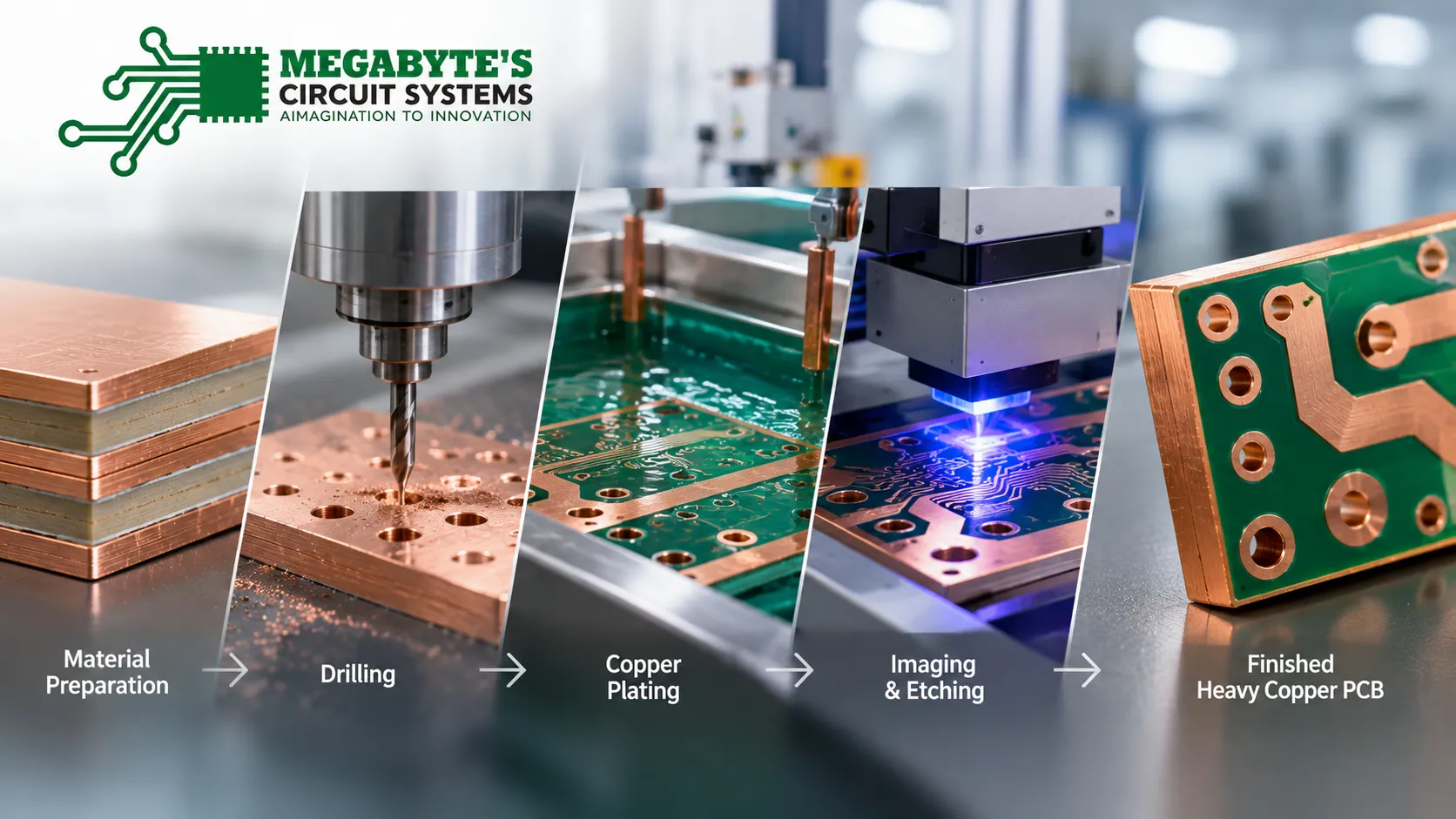
The fabrication of heavy copper PCBs differs significantly from standard boards. Here is how we handle it at our PCB manufacturing facility in Ahmedabad.
We start with high-Tg FR-4 laminates (Tg 170°C or higher) rated for the thermal stress of heavy copper processing. The stackup is planned carefully, balancing copper weights across layers to minimize warpage. For a 6 oz inner layer, the prepreg and core thicknesses must compensate for copper volume during lamination.
Unlike standard PCBs that use 1 oz copper and simple etching, heavy copper boards require differential etching or pattern plating techniques. Plating up to the target copper thickness (3 oz to 10 oz) is done through electrolytic copper deposition. Etch factors must be carefully controlled because thick copper undercuts more aggressively. A 6 oz copper layer can experience lateral etch of 150 µm to 200 µm per side.
Heavy copper multilayer boards require higher lamination pressures and modified press cycles. The resin fill must completely encapsulate the thick copper features without voids. This is where experience matters. We use programmed press cycles with controlled ramp rates to avoid resin starvation between heavy copper traces.
Drilling through thick copper layers demands higher spindle speeds and specialized drill bits to avoid burring. The plated through-hole (PTH) barrels must handle the current requirements, so minimum hole wall plating is typically 25 µm or more, exceeding the IPC Class 2 minimum of 20 µm.
Heavy copper boards undergo electrical testing (E-test) and thermal stress testing. Solder mask application requires multiple coats to build sufficient thickness over tall copper features. We use flying probe testing on every heavy copper panel to verify net connectivity.
Quick Technical Summary: Heavy copper PCB fabrication requires differential etching, high-Tg laminates, controlled lamination press cycles, and specialized drilling. Lateral etch of 150 to 200 µm per side on 6 oz copper makes tight trace/space designs challenging, requiring minimum 200 µm (8 mil) trace widths.
One thing I always tell my clients is this: these two technologies solve different problems. Choosing between them depends on your specific thermal, electrical, and mechanical requirements. Here is a detailed comparison.
Parameter | Heavy Copper PCB | Metal Core PCB (MCPCB) |
Base Material | FR-4 (standard or high-Tg) | Aluminum or copper metal base |
Copper Weight | 3 oz to 20 oz/ft² | 1 oz to 3 oz (circuit layer) |
Thermal Conductivity | 0.25 W/m·K (FR-4 substrate) | 1.0 to 8.0 W/m·K (dielectric) |
Current Carrying Capacity | Very high (50A to 200A per trace) | Moderate (standard trace widths) |
Layer Count | Single to 16+ layers possible | Mostly single layer, some double layer |
Typical Thickness | 1.6 mm to 6.0 mm | 1.0 mm to 3.2 mm |
Heat Dissipation Method | Through copper planes and thermal vias | Through metal base acting as heatsink |
Primary Applications | Power supplies, EV, military, motor drives | LED lighting, automotive lights, RF amplifiers |
Cost (Relative) | Higher (due to copper and processing) | Lower for single-layer designs |
Design Complexity | Supports complex multilayer routing | Limited to 1 to 2 layers typically |
When to choose heavy copper: Your design needs to carry high currents (above 10A per trace), requires multilayer routing, or must survive extreme thermal cycling. Common in EV battery management, power converters, and defense electronics.
When to choose MCPCB: Your primary concern is spreading heat from surface-mounted components (like LEDs or power MOSFETs) across the board. You need a cost-effective thermal solution and single-layer routing is sufficient.
For projects that need both high current and metal-core thermal management, we sometimes fabricate hybrid boards with heavy copper layers on a metal base. Talk to our engineering team if your design falls in this category.
The electric vehicle industry is one of the fastest-growing markets for heavy copper PCBs for EV applications. Battery management systems (BMS), onboard chargers (OBC), DC-DC converters, and motor inverters all require copper weights of 4 oz to 10 oz to handle continuous currents of 30A to 150A.
We see this demand increasing every quarter from Indian EV manufacturers. A well-designed heavy copper multilayer PCB with 6 oz copper, proper thermal vias, and adequate creepage distances can reliably serve in a 400V EV powertrain environment.
The LED PCB board market relies almost entirely on MCPCB technology. An aluminum-based MCPCB keeps LED junction temperatures below the critical threshold (typically 85°C to 120°C), directly extending LED lifespan from 25,000 hours to 50,000+ hours.
For high-power LED arrays (50W to 500W), we recommend aluminum MCPCBs with a dielectric thermal conductivity of at least 2.0 W/m·K. Standard single layer PCBs on FR-4 simply cannot handle the thermal load of high-power LED modules.
Power supplies, welding machines, UPS systems, and solar inverters frequently use heavy copper boards. A 4-layer board with 4 oz copper on the power layers and 1 oz on the signal layers is a very common configuration we produce for industrial clients.
Quick Technical Summary: Heavy copper PCBs dominate EV powertrains (BMS, OBC, inverters) handling 30A to 150A continuously, while MCPCBs are the standard for LED lighting where junction temperature control extends lifespan to 50,000+ hours. Industrial power electronics often use hybrid stackups with mixed copper weights.
Getting your design right before sending Gerber files saves time, money, and frustration. Here are the most important Design for Manufacturing rules I share with every client.
Getting your design right before sending Gerber files saves time, money, and frustration. Here are the most important Design for Manufacturing rules I share with every client.
Quick Technical Summary: Heavy copper DFM requires wider traces (6 to 10 mil minimum depending on copper weight), increased spacing, generous thermal vias, and balanced copper on all layers. MCPCB designs should specify dielectric thickness precisely and avoid unnecessary through-holes.
At Megabyte Circuit Systems, every heavy copper and MCPCB panel goes through a rigorous quality process aligned with international standards.
We test to IPC-6012 Class 2 and Class 3 specifications depending on the application. For heavy copper boards going into EV or defense projects, Class 3 is mandatory, requiring minimum 25 µm hole wall copper plating and tighter annular ring tolerances.
Our quality process includes AOI (Automated Optical Inspection) for every layer before lamination, flying probe electrical testing on 100% of panels, cross-section analysis for plating thickness verification, and thermal stress testing (288°C solder float for 10 seconds per IPC-TM-650).
For MCPCB, we verify dielectric breakdown voltage (minimum 3 kV for standard aluminum MCPCBs), thermal conductivity of the dielectric layer, and peel strength of the copper circuit layer (minimum 1.0 N/mm per IPC-4101).
Soldering quality on assembled boards follows IPC-A-610 Class 2 or Class 3 and J-STD-001 workmanship standards. We see this attention to testing as non-negotiable, especially for power and automotive applications where field failures are costly and dangerous.
Let me be straightforward. Heavy copper PCBs are more expensive than standard boards. The extra copper material, longer plating cycles, and specialized processing all add cost. But there are smart ways to optimize.
Optimize copper weight by layer. You don’t need 6 oz copper on every layer. Use heavy copper (4 to 6 oz) only on power layers and standard 1 oz on signal layers. This hybrid approach can reduce cost by 20% to 30% compared to uniform heavy copper across all layers.
Panel utilization matters. Work with your fabricator to fit the maximum number of boards per panel. A small change in board outline dimensions can sometimes add one or two extra pieces per panel, reducing per-unit cost significantly.
For MCPCBs, aluminum is much cheaper than copper base. Unless your thermal requirements specifically demand a copper base (thermal conductivity of 380 W/m·K vs. 200 W/m·K for aluminum), stick with aluminum. The cost difference can be 3x to 5x.
Order in production quantities. Both heavy copper and MCPCB setups involve significant tooling and process time. Ordering 50 to 100 pieces is far more cost-efficient per unit than ordering 5 prototypes. Use our PCB calculator to compare pricing across different quantities instantly.
Choose an Indian MCPCB manufacturer. Sourcing from a domestic MCPCB manufacturer in India like Megabyte Circuit Systems eliminates import duties, reduces lead times from 4 to 6 weeks (international) down to 7 to 12 working days, and makes communication and revision cycles much faster.
Quick Technical Summary: Heavy copper cost can be reduced 20% to 30% by using mixed copper weights across layers. Aluminum MCPCB is 3x to 5x cheaper than copper-base MCPCB. Domestic Indian sourcing cuts lead times to 7 to 12 days and eliminates import overhead.
A heavy copper PCB uses thick copper layers (3 oz and above) on a standard FR-4 substrate to carry high current. An MCPCB uses a metal base (aluminum or copper) with a thermally conductive dielectric for heat spreading. Heavy copper excels at current handling, while MCPCB excels at thermal dissipation from surface components like LEDs.
Any copper weight of 3 oz/ft² (105 µm) or above is classified as heavy copper. Standard PCBs use 1 oz (35 µm) to 2 oz (70 µm). Extreme heavy copper can go up to 20 oz/ft² (700 µm) for specialized applications like bus bars and high-power distribution.
Most MCPCBs are single-layer designs. Double-layer MCPCBs are available but more complex and expensive. Multilayer MCPCBs beyond two layers are extremely rare and difficult to manufacture because the metal core complicates via formation and interlayer registration.
Heavy copper PCB is the preferred choice for EV applications. EV systems like BMS, motor inverters, and DC-DC converters require high current capacity (30A to 150A) and multilayer routing, which heavy copper on FR-4 handles far better than single-layer MCPCB.
At Megabyte Circuit Systems, standard lead time for heavy copper PCBs is 10 to 15 working days depending on copper weight, layer count, and order quantity. MCPCBs are typically faster at 7 to 12 working days. Rush orders can be accommodated with prior discussion.
LED PCB boards almost universally use aluminum-based MCPCB with a thermally conductive dielectric layer. The aluminum base (typically 5052 or 6061 alloy) acts as an integrated heatsink, keeping LED junction temperatures within safe operating limits.
Heavy copper PCBs and MCPCBs are both specialized technologies designed for demanding thermal and electrical environments. The right choice depends on whether your primary need is high current capacity (heavy copper) or efficient thermal spreading (MCPCB). Understanding the construction, design rules, and manufacturing constraints of each technology will save you from costly redesigns.
At Megabyte Circuit Systems in Ahmedabad, Gujarat, we manufacture both heavy copper PCBs (up to 10 oz) and aluminum MCPCBs with fast turnaround and full quality testing to IPC standards. Whether you are building an EV powertrain, an LED lighting module, or an industrial power supply, our team is ready to help.
Upload your Gerber files today, get an instant estimate using our PCB calculator, or reach out to our engineering team for a custom quote. Let’s build something reliable together.
C/10, Yogeshwar Estate, B/H Madhuram Estate, Nr. Vishala Estate, Sardar Patel Ring Rd, Odhav, Ahmedabad, Gujarat, Ahmedabad - 382430, Gujarat (India)
Copyright © 2025. Megabytes Circuit Systems All rights reserved.
Powered by FrogMEE Tech