Ahmedabad - 382430, Gujarat (India)

Every PCB that leaves a production line carries a risk. A single undetected open circuit, a misaligned component, or a hairline solder bridge can turn a finished product into a warranty claim. Choosing the right pcb testing methods is not just a quality checkbox. It is the difference between shipping confidently and shipping with your fingers crossed.
This guide breaks down the four most widely used PCB testing and inspection methods: AOI (Automated Optical Inspection), ICT (In-Circuit Testing), Flying Probe Testing, and Functional Testing. I will walk you through how each one works, what faults it catches, where it falls short, and when to use it. At Megabyte Circuit Systems, we run thousands of boards through these processes every month at our Ahmedabad facility, and I will share the practical insights we have gathered over 20+ years.
By the end, you will know exactly which testing strategy fits your volume, budget, and reliability requirements.
PCB testing is the systematic process of verifying that a printed circuit board meets its design specifications, is free from manufacturing defects, and will perform reliably in its intended application. It covers everything from visual solder joint inspection to full electrical verification of circuit behavior.
Here is why it matters in real numbers. Industry data shows that catching a defect at the bare board stage costs roughly ₹5 to ₹15 per board. Catching the same defect after assembly costs ₹200 to ₹500. If that defect reaches the field, the cost jumps to ₹2,000 or more when you factor in returns, rework, and reputation damage. Testing is not an expense. It is the cheapest insurance your project has.
The IPC-A-610 standard (Acceptability of Electronic Assemblies) and IPC-6012 (Qualification and Performance Specification for Rigid PCBs) define the acceptance criteria that professional pcb quality inspection processes follow. Every testing method we discuss below maps back to these benchmarks.
Quick Technical Summary: PCB testing verifies design conformance and detects manufacturing defects before boards ship. Catching defects early at the board level is 10x to 100x cheaper than catching them in the field. IPC-A-610 and IPC-6012 set the industry-standard acceptance criteria.
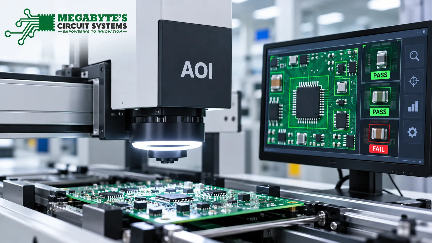
AOI (Automated Optical Inspection) is a non-contact, camera-based inspection method that uses high-resolution imaging and pattern-matching algorithms to detect surface-level defects on PCBs. It is the fastest visual inspection method available in modern electronics manufacturing.
An AOI machine captures images of the board from multiple angles using LED lighting systems and high-resolution cameras (typically 10 to 15 megapixels). The system compares each captured image against a reference image (golden board) or CAD data to identify deviations.
AOI cannot see hidden solder joints under BGA (Ball Grid Array) packages. It cannot verify electrical connectivity or measure resistance values. For BGA inspection, X-ray inspection is required. Also, AOI generates false calls on highly reflective or unusually shaped components, which means an operator must review flagged boards.
A typical AOI system inspects at speeds of 25 to 60 cm² per second, making it ideal for 100% inline inspection on high-volume production lines. We use AOI as a standard step in our PCB assembly service process at Megabyte.
Quick Technical Summary: AOI uses high-resolution cameras and pattern matching to detect surface-level defects at speeds of 25 to 60 cm² per second. It excels at catching solder and component placement errors but cannot inspect hidden joints under BGAs or verify electrical functionality.
ICT (In-Circuit Testing) is an electrical testing method that uses a bed-of-nails fixture to make contact with specific test points on a populated PCB, allowing it to measure individual component values, verify connectivity, and check for shorts and opens.
A custom fixture with spring-loaded probes (the “bed of nails”) is built to match the board’s test point layout. When the board is placed on the fixture, each probe contacts a designated pad. The system then runs a sequence of electrical measurements.
The main drawback of ICT is the fixture cost. A custom bed-of-nails fixture typically runs ₹80,000 to ₹3,00,000+ depending on board complexity. This makes ICT economical only for production volumes above 500 to 1,000 units. For prototype runs or small batches, the per-unit fixture amortization makes it prohibitively expensive.
ICT achieves electrical test coverage of 85% to 95% of a board’s nets and is the gold standard for medium to high volume production. One thing I always tell my clients is this: if your annual volume exceeds 1,000 boards and your design is stable, invest in an ICT fixture. The per-board cost drops below ₹10 to ₹25, and the fault coverage is hard to beat.
Quick Technical Summary: ICT uses a custom bed-of-nails fixture to electrically test individual components and connections. It offers 85% to 95% fault coverage but requires ₹80,000 to ₹3,00,000+ in fixture costs, making it most economical for volumes above 500 to 1,000 units.
Flying probe testing is a fixtureless electrical testing method where motorized probes move across the board, contacting test points sequentially to check for opens, shorts, resistance, capacitance, and diode orientation.
Instead of a fixed fixture, two to eight motorized probes (depending on the machine) navigate to test points using coordinates from the board’s CAD/netlist data. The probes contact each point one pair at a time, running the programmed electrical measurements.
The biggest advantage of flying probe is zero fixture cost. Programming a new board takes 1 to 4 hours, compared to weeks for an ICT fixture. This makes it ideal for prototypes, engineering validation (EVT) builds, and low-to-medium volume production.
At Megabyte Circuit Systems, flying probe is our go-to method for customers ordering prototype and small batch runs. When a startup sends us a new double layer PCB design for the first time, flying probe lets us verify every net without any tooling investment.
Flying probe is significantly slower than ICT. A board that takes 5 to 10 seconds on an ICT fixture may take 2 to 15 minutes on a flying probe, depending on net count. For a complex multilayer PCB with 3,000+ nets, test times can exceed 20 minutes per board. This makes it impractical as the sole test method for volumes above 1,000 to 2,000 units.
Modern flying probe machines achieve positional accuracy of ±0.015mm and can test component values with measurement accuracy within ±0.5% for resistance.
Quick Technical Summary: Flying probe testing uses motorized probes with zero fixture cost and ±0.015mm positional accuracy. It is ideal for prototypes and small batches (under 1,000 units) but is too slow for high-volume production due to sequential point-by-point testing.
Functional testing (FCT) verifies that a fully assembled PCB operates correctly as a complete system by simulating real-world operating conditions, including power-up sequences, signal inputs, and load responses.
The board is connected to a custom test jig that supplies power, input signals, and simulated loads. The system then monitors output signals, voltages, current draw, timing, and communication protocols (UART, SPI, I2C, CAN) to confirm the board behaves as designed.
While AOI, ICT, and flying probe focus on detecting manufacturing defects, functional testing validates design performance. A board can pass ICT perfectly (all components correct, all nets connected) and still fail functionally due to firmware bugs, signal integrity issues, or thermal behavior.
In my experience, functional testing catches roughly 5% to 10% of issues that slip past all other methods. These are often subtle timing errors, power sequencing problems, or edge-case failures that only appear under real operating conditions.
Functional test development costs vary widely, from ₹20,000 for a simple power-on and communication check to ₹5,00,000+ for a comprehensive test covering multiple operating modes. The test jig is typically application-specific.
Quick Technical Summary: Functional testing validates that a fully assembled PCB performs correctly under simulated real-world conditions. It catches design-level and system-level issues (5% to 10% of total defects) that component-level tests like ICT and flying probe cannot detect.
Parameter | AOI | ICT | Flying Probe | Functional Testing |
Test Type | Visual/Optical | Electrical | Electrical | System-Level |
Fixture Required | No | Yes (Bed-of-Nails) | No | Yes (Custom Jig) |
Fixture/Setup Cost | Nil | ₹80,000 to ₹3,00,000+ | Nil (programming only) | ₹20,000 to ₹5,00,000+ |
Fault Coverage | Surface defects only | 85% to 95% electrical | 80% to 90% electrical | Application-specific |
Test Speed | 5 to 20 sec/board | 5 to 30 sec/board | 2 to 20 min/board | 30 sec to 10 min/board |
Best For | High volume, 100% inline | Medium to high volume (500+) | Prototypes, small batch | Final validation, all volumes |
Cannot Detect | Hidden joints, electrical faults | Functional/system errors | High-speed signal issues | Individual component faults |
Ideal Volume | All volumes | 500+ units | 1 to 500 units | All volumes |
How to read this table: For prototype and low-volume production, combine flying probe with functional testing. For medium volume, add AOI as an inline screen before ICT. For high volume, use the full chain: AOI → ICT → Functional Test. There is no single method that catches everything, which is why professional PCB manufacturing services layer multiple methods together.
Designing your board for testability from the start saves significant cost and time during production. Here are the rules we follow at Megabyte:
You can use our PCB calculator to get instant estimates for boards designed with proper test accessibility.
Quick Technical Summary: Design for testability (DFT) requires minimum 1.0mm test pads with 1.27mm spacing, test points on one side, and 50 mils clearance from edges. Providing complete design files (Gerber, BOM, netlist, centroid) eliminates test programming delays.
Every board at Megabyte goes through a structured quality process aligned with international IPC standards:
Bare board testing per IPC-6012 Class 2 (or Class 3 for defense and medical applications) includes continuity/isolation testing using our flying probe testers with 100% net coverage. Visual inspection follows IPC-A-600 criteria for surface quality, hole wall integrity, and plating thickness.
Assembled board testing follows IPC-A-610 acceptance criteria for solder joint quality. Our AOI systems inspect every assembled board before electrical testing. For complex boards, especially single layer PCBs used in high-reliability applications and multilayer stacks for IoT gateways, we apply the appropriate test combination based on volume and criticality.
We see this issue very often with first-time customers: they submit boards with no test points, no netlist, and expect full electrical verification. Starting the DFT conversation early, ideally during our PCB design service phase, prevents costly redesigns later.
Testing costs in India are significantly lower than in Western markets, but smart choices can reduce them further:
Choose the right method for your volume. Do not invest in an ICT fixture for a 50-piece prototype run. Use flying probe instead and save ₹1,00,000+ in tooling.
Combine AOI with one electrical method. AOI as a pre-screen catches obvious assembly defects before expensive electrical testing. This reduces ICT/flying probe test time because fewer defective boards enter the electrical test stage.
Optimize test point placement during design. Boards designed with proper test access reduce fixture complexity and programming time. This directly lowers per-unit test cost by 15% to 25%.
Consolidate testing with your manufacturer. When your PCB fabrication, assembly, and testing happen under one roof (as they do at Megabyte), you eliminate shipping between vendors, reduce handling damage, and get faster turnaround.
Get an instant estimate for your project, including testing, using our PCB calculator.
Quick Technical Summary: Matching your test method to production volume is the single biggest cost lever. Flying probe for prototypes, AOI + ICT for volume, and consolidating fabrication, assembly, and testing with one manufacturer reduces total cost by eliminating inter-vendor logistics.
AOI (Automated Optical Inspection) is the most widely used PCB testing method globally. It is deployed on nearly every SMT production line for 100% inline visual inspection. For electrical testing, ICT is the most common for high-volume production, while flying probe dominates prototype and low-volume work.
Costs vary by method and volume. Flying probe testing typically costs ₹50 to ₹300 per board for small batches. ICT costs ₹10 to ₹25 per board at volume but requires ₹80,000 to ₹3,00,000+ in fixture investment. AOI adds ₹5 to ₹15 per board when included in an assembly line.
For prototype and low-volume production (under 500 units), yes. Flying probe provides comparable electrical fault coverage of 80% to 90%. However, for volumes above 1,000 units, ICT is faster and more cost-effective per board. The two methods are complementary, not interchangeable at all volumes.
AOI cannot detect hidden solder joints under BGA packages, electrical opens that appear visually normal, incorrect component values (a 10kΩ resistor looks identical to a 100kΩ resistor), and functional or firmware-related issues. X-ray inspection and electrical testing methods cover these gaps.
IPC-A-610 governs acceptability of electronic assemblies including solder joint criteria. IPC-6012 covers qualification and performance of rigid printed boards. IPC-A-600 covers acceptability of printed boards (bare board visual criteria). J-STD-001 covers soldering process requirements.
For safety-critical applications (medical, automotive ADAS, defense, aerospace), 100% electrical testing per IPC-6012 Class 3 is mandatory. For commercial consumer electronics (Class 2), statistical sampling combined with AOI may be acceptable depending on defect rates and risk tolerance.
If your production volume is above 500 units and the design is finalized, ICT is more economical. If you are in prototyping, running multiple design revisions, or producing under 500 units, flying probe avoids fixture costs and offers faster turnaround.
Choosing the right PCB testing methods comes down to three factors: your production volume, your defect risk tolerance, and your budget. No single method covers everything. The most reliable approach layers visual inspection (AOI) with electrical verification (ICT or flying probe) and functional validation, matched to your specific production stage.
At Megabyte Circuit Systems in Ahmedabad, Gujarat, we help you select the right testing combination during the quoting stage itself, so there are no surprises during production. Whether you need bare board verification for a prototype or full AOI + ICT + functional testing for a volume run, we handle it all under one roof.
Ready to get started? Upload your Gerber files, use our PCB calculator for an instant estimate, or contact our team to discuss the right testing strategy for your next project.
C/10, Yogeshwar Estate, B/H Madhuram Estate, Nr. Vishala Estate, Sardar Patel Ring Rd, Odhav, Ahmedabad, Gujarat, Ahmedabad - 382430, Gujarat (India)
Copyright © 2025. Megabytes Circuit Systems All rights reserved.
Powered by FrogMEE Tech