Ahmedabad - 382430, Gujarat (India)

If you’re a hardware engineer or an IoT startup founder in India, you already know the drill. You’ve spent weeks perfecting your schematic, routing your traces, and running DRCs. Now comes the stressful part: sending those files off to a fab house and praying the boards come back right.
In my 20+ years at Megabyte Circuit Systems, I’ve personally guided hundreds of electronics teams through this exact transition. Let’s be honest—relying on overseas fabricators used to be the default. But with rising shipping costs, unpredictable customs holds, and a massive push for localized supply chains, executing an online pcb order in India is now faster, highly cost-effective, and technically superior if you partner with the right fab.
Whether you need a quick-turn prototype or a full-scale production run, figuring out how to buy pcb online shouldn’t be a guessing game. In this guide, I’m going to sit down with you and walk through the exact step-by-step process to get your custom pcb online india order placed flawlessly, ensuring your boards are manufactured exactly to your specifications.
To successfully buy a PCB online, you must export your design into industry-standard formats like Gerber RS-274X or ODB++. A complete package includes copper layers, solder mask, silkscreen, mechanical outlines, and Excellon drill files. Missing or misaligned drill files are the #1 cause of manufacturing delays.
Before you can order anything, we need your manufacturing data. Your EDA software (Altium, KiCad, Eagle) speaks one language, but our factory floor machinery speaks another.
One thing I always tell my clients is: never assume your fab house knows what you meant. You need to explicitly define every layer. Generate standard Gerber RS-274X or ODB++ files. Make sure your ZIP file contains:
Pro Tip from the Fab Floor: Always include a simple ReadMe.txt file in your Gerber ZIP. State your required board thickness, copper weight, and any special impedance requirements. It takes you two minutes but saves us hours of engineering queries.
Selecting the correct board parameters dictates both the electrical performance and the cost of your PCB. Standardizing on 1.6mm FR-4 with 1oz copper and green solder mask provides the fastest lead times. High-speed designs require specific dielectric constants and impedance-controlled stack-ups.
Once your files are ready, you need to define the physical characteristics of your board. When you place an online pcb order in India, the default parameters are usually 1.6mm FR-4, 1oz (35µm) copper, HASL Lead-Free finish, and green solder mask. Deviating from these standard specs can increase costs and lead times.
Here is how you should think about layer counts based on your application:
Modern Indian PCB manufacturers offer automated quoting tools where you input board dimensions, layers, and quantities. This eliminates back-and-forth emails and provides transparent, real-time pricing. For complex builds, engineering review is still necessary before final payment.
Gone are the days when you had to send an email with your Gerber files and wait 48 hours for a sales rep to reply. To buy pcb online efficiently, you should use an automated system.
At Megabyte, we’ve built a dedicated tool to make this frictionless. You can simply use our PCB Calculator to input your board dimensions (Length x Width), select your quantity, choose your layer count, and get an instant cost estimate. This transparency helps procurement managers budget accurately for prototypes and production runs alike.
If your board requires advanced features like blind/buried vias, castellations, or specific dielectric materials (like Rogers), you can upload your files directly through the portal for our CAM engineers to run a custom DFM analysis.
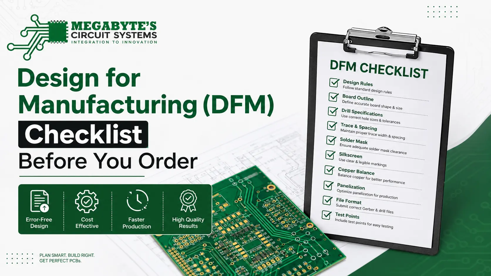
DFM checks ensure your board can actually be built without defects. Key checks include maintaining minimum trace widths, adequate annular ring sizes, and proper copper-to-edge clearances. Catching these errors before ordering prevents acid traps, shorts, and costly respins.
I’ve seen hundreds of brilliant designs fail on the manufacturing floor because the engineer ignored factory capabilities. Before you hit “Order”, run through this quick DFM checklist:
\[ Z_0=\frac{87}{\sqrt{\varepsilon_r+1.41}} \ln\left(\frac{5.98h}{0.8w+t}\right) \]
Always leave a note if you need us to adjust trace widths on our end to hit your target impedance.
Understanding the difference between standard capabilities (low cost, fast turn) and advanced capabilities (higher cost, longer lead time) helps engineers optimize their designs. Always design to standard specs unless the circuit absolutely demands advanced parameters.
To help you decide what specs to select during your online checkout, here is a quick reference table of standard vs. advanced manufacturing capabilities:
Feature | Standard Capability (Fastest/Cheapest) | Advanced Capability (Higher Cost) |
Material | Standard FR-4 (TG 130-140) | High-TG FR-4 (TG 170+), Rogers, Polyimide |
Min Trace/Space | 5 mil / 5 mil | 3 mil / 3 mil (or tighter) |
Min Drill Size | 0.3 mm (Mechanical) | 0.1 mm (Laser via) |
Surface Finish | HASL (Lead-Free) | ENIG, Hard Gold, Immersion Silver |
Via Types | Through-hole Vias | Blind, Buried, Microvias (HDI) |
Ordering custom PCBs locally in India eliminates unpredictable customs delays, high international shipping costs, and communication barriers. Local fabricators adhere to global IPC standards and provide rapid prototyping support directly aligned with the “Make in India” initiative.
There was a time when looking for a custom pcb online india vendor meant compromising on quality or paying a massive premium. That is no longer true.
When you choose a dedicated domestic partner for PCB Manufacturing, you are eliminating the most painful bottlenecks in hardware development. You don’t have to worry about your prototypes sitting in customs for a week. You don’t have to deal with time-zone lags when a CAM engineer has a question about a short circuit in your Gerber files.
At Megabyte Circuit Systems in Ahmedabad, we manufacture strictly to IPC-A-600 Class 2 and Class 3 standards. Every board goes through automated optical inspection (AOI) and rigorous electrical E-testing (Flying Probe) before it leaves our facility. We give you factory-direct communication, ensuring that if there’s an issue with your design, you hear about it from a senior engineer immediately—not after the boards have already been ruined.
Standard lead times for prototype double-layer PCBs range from 5 to 7 working days. If you require expedited service, quick-turn manufacturing can bring this down to 48–72 hours, depending on the complexity of the board.
For prototyping, there is usually no strict MOQ, though most online calculators default to a minimum of 5 pieces. This allows engineers to test their designs cost-effectively before committing to high-volume production.
Reputable manufacturers run a Design for Manufacturing (DFM) check before processing payment or starting production. At Megabyte, our CAM engineers review your files for DRC errors, drill misalignments, and clearance issues to ensure the board is 100% manufacturable.
For standard through-hole and general SMD components, Lead-Free HASL is the most cost-effective. However, if your board has fine-pitch components like BGAs or QFNs, you should select ENIG (Electroless Nickel Immersion Gold) for a perfectly flat soldering surface.
Yes, once your order is confirmed and pushed to the factory floor, you will receive updates throughout the manufacturing stages (drilling, plating, masking, testing) and a tracking number once the boards are dispatched.
Navigating hardware development is hard enough without having to worry about manufacturing errors or shipping delays. By utilizing local, high-quality fabrication, you gain total control over your project timeline and budget.
If you have a design ready to go, don’t leave it sitting on your hard drive. Head over to our PCB Calculator right now, plug in your specs, and get an instant quote.
Upload your Gerbers, and let’s get your boards onto the factory floor today. If you have any specific technical requirements or need help optimizing your design for manufacturing, our engineering team in Ahmedabad is just a phone call away. Let’s build something great together.
C/10, Yogeshwar Estate, B/H Madhuram Estate, Nr. Vishala Estate, Sardar Patel Ring Rd, Odhav, Ahmedabad, Gujarat, Ahmedabad - 382430, Gujarat (India)
Copyright © 2025. Megabytes Circuit Systems All rights reserved.
Powered by FrogMEE Tech