Ahmedabad - 382430, Gujarat (India)
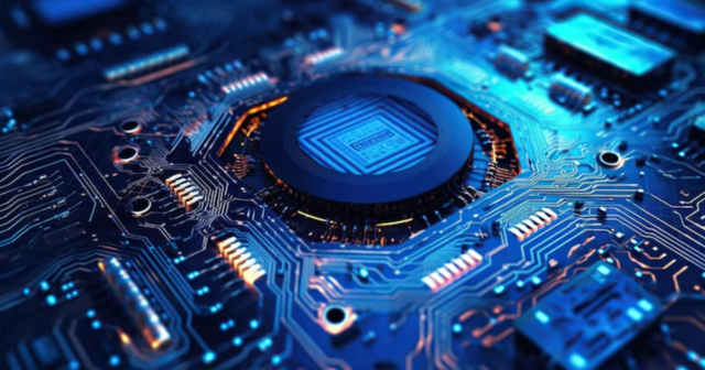
PCB fabrication is the process of creating a printed circuit board (PCB) by designing and manufacturing its foundational structure, which includes layers of insulating material, copper traces, and drilled holes, before components are added. It’s the critical first step in producing the boards that power nearly every electronic device, from smartphones to medical equipment. Unlike PCB assembly, which focuses on attaching components, fabrication builds the bare board itself, setting the stage for reliable functionality. In this guide, we’ll explore the PCB fabrication process, its stages, materials, technologies, and best practices to help engineers, hobbyists, and manufacturers understand this essential process.
PCB fabrication involves designing and constructing the physical structure of a printed circuit board, which serves as the backbone for electronic circuits. The process starts with a schematic design and transforms it into a tangible board made of insulating materials like fiberglass (FR-4) and conductive copper layers. These boards feature etched copper traces for electrical connectivity, drilled holes for component leads, and a protective solder mask. Fabrication ensures the board is ready for the next step PCB assembly where components are mounted to create a functional circuit.
The PCB fabrication process is a series of precise steps that transform a design into a physical board. Below, we outline the key stages involved.
The process begins with PCB design, where engineers create a schematic diagram outlining the circuit’s electrical connections. Using software like Altium Designer or KiCad, they convert the schematic into a PCB layout, defining the placement of components, copper traces, and vias. This layout is exported as Gerber files, which contain the data needed for manufacturing, including layer information, drill locations, and board dimensions.
The foundation of a PCB is its substrate, typically a fiberglass material like FR-4, which provides insulation and mechanical strength. Other materials, such as polyimide for flexible PCBs or ceramic for high-temperature applications, may be used depending on the board’s requirements. Copper foil is laminated onto the substrate to form conductive layers, with the thickness (e.g., 1 oz or 2 oz per square foot) chosen based on current-carrying needs.
The PCB design is transferred onto the copper-clad board through a process called imaging. A photoresist layer is applied to the board, and the Gerber files guide a laser or UV light to expose the circuit pattern. The unexposed photoresist is washed away, leaving the desired pattern. Next, an etching solution (like ferric chloride) removes the unwanted copper, leaving behind the copper traces that form the circuit.
For multilayer PCBs, several layers of prepreg (a resin-soaked fiberglass sheet) and copper-clad cores are stacked and bonded under heat and pressure in a lamination process. This creates a single, cohesive board with internal copper layers connected by vias. Multilayer boards are common in complex devices like computers, where high-density circuits are required.
Holes are drilled into the board to accommodate component leads (for through-hole technology) and vias (for interlayer connections). High-precision CNC drilling machines use the Gerber drill files to ensure accuracy. For multilayer boards, vias may be plated with copper to establish electrical connections between layers, a process known as via plating.
After drilling, the board undergoes copper plating to reinforce the vias and pads. A surface finish, such as HASL (Hot Air Solder Leveling), ENIG (Electroless Nickel Immersion Gold), or OSP (Organic Solderability Preservative), is applied to protect the copper from oxidation and improve solderability during assembly. The choice of finish depends on the board’s application and assembly requirements.
A solder mask, typically green but available in other colors, is applied to insulate the copper traces and prevent solder bridges during assembly. It also protects the board from environmental damage. The silkscreen layer adds labels, component outlines, and identifiers (e.g., part numbers) using ink, aiding in assembly and troubleshooting.
Before the board is shipped, it undergoes electrical testing to verify continuity and detect shorts or opens. Common methods include the flying probe test, which uses probes to check connections, and the bed-of-nails test, which uses a fixture to test multiple points simultaneously. This ensures the fabricated board meets design specifications and is ready for assembly.
PCBs come in various types, each suited to specific applications.
Single-layer PCBs have copper traces on only one side of the substrate, making them the simplest and most affordable option. They’re ideal for basic electronics like LED circuits or power supplies but lack the capacity for complex circuits.
Double-layer PCBs feature copper traces on both sides of the substrate, connected by vias. They offer more design flexibility and are used in applications like amplifiers or consumer electronics, where moderate complexity is needed.
Multilayer PCBs have three or more layers of copper traces, separated by insulating layers and connected by vias. They’re essential for advanced devices like smartphones, servers, and medical equipment, where high-density circuits and signal integrity are critical.
The choice of materials in PCB fabrication impacts the board’s performance, durability, and cost.
PCB fabrication isn’t without challenges. Common issues include:
Modern PCB fabrication has evolved with technologies that enhance precision and functionality.
To ensure a successful fabrication process, follow these best practices:
While often confused, PCB fabrication and assembly are distinct processes. Fabrication creates the bare board, focusing on the layout, materials, and structure. Assembly, or PCBA, follows fabrication and involves mounting components onto the board using soldering techniques like SMT or THT. Fabrication sets the foundation, while assembly brings the board to life with functional circuitry.
PCB fabrication is the cornerstone of modern electronics, enabling the creation of compact, reliable, and efficient devices. From consumer gadgets to aerospace systems, fabricated PCBs ensure that circuits can handle the demands of advanced technology. As devices become smaller and more complex, innovations in fabrication like HDI and flexible PCBs continue to push the boundaries of what’s possible.
PCB fabrication is a meticulous process that transforms a design into a functional board, laying the groundwork for reliable electronics. By understanding its stages design, material selection, etching, lamination, drilling, and testing you can appreciate the precision required to create high-quality PCBs. Whether you’re designing a simple single-layer board or a complex multilayer HDI PCB, mastering fabrication ensures your electronics perform at their best.
C/10, Yogeshwar Estate, B/H Madhuram Estate, Nr. Vishala Estate, Sardar Patel Ring Rd, Odhav, Ahmedabad, Gujarat, Ahmedabad - 382430, Gujarat (India)
Copyright © 2025. Megabytes Circuit Systems All rights reserved.
Powered by FrogMEE Tech