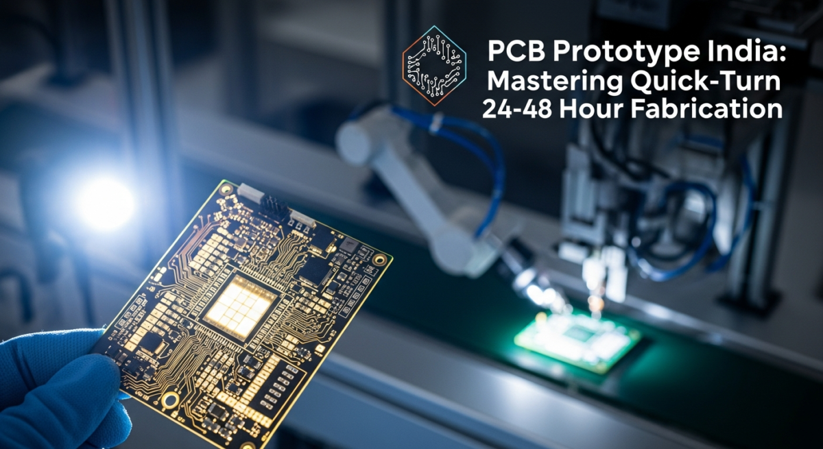
PCB Prototype India: Mastering Quick-Turn 24-48 Hour Fabrication
In the high-stakes world of electronic product development, the bridge between a schematic and a functional hardware product is the prototype. For Indian hardware engineers and IoT startups, time-to-market is the ultimate KPI. A delay in receiving a pcb prototype India can mean missing a venture capital milestone or a critical product launch window.
At Megabyte Circuit Systems, we recognize that “fast” isn’t just about shipping speed; it’s about the technical precision of the quick-turn prototyping process. Whether you are developing a Single Layer PCB for a power supply or a complex Multilayer PCB for an AI-on-the-edge device, your prototype serves as the definitive proof of concept. This guide explores the technical parameters, manufacturing standards, and speed-optimized workflows that define the fastest PCB prototype India services in 2026.
The Anatomy of a Quick-Turn PCB Prototyping Process
Quick Technical Summary: The quick-turn PCB prototyping process compresses traditional 14-day manufacturing cycles into 24–48 hours by utilizing high-speed digital imaging (LDI) and automated CAM validation. This workflow eliminates physical tooling delays, allowing for immediate transition from Gerber files to the etching stage.
When an engineer searches for a pcb prototype India, they are typically looking for an agile response to design iterations. The process at Megabyte begins with an automated CAM (Computer-Aided Manufacturing) review. As soon as you upload your Gerber files (RS-274X or ODB++ formats), our engineers perform a netlist comparison to ensure the physical board will match your electrical intent.
The manufacturing stages for an urgent prototype include:
- LDI (Laser Direct Imaging): Instead of creating film phototools, we use lasers to scan the circuit pattern directly onto the photoresist-coated copper. This is essential for maintaining a tight trace width and spacing (down to 4/4 mil).
- PTH (Plated Through Hole) Processing: For a Double Layer PCB, we utilize high-speed electrolysis to deposit copper in the drilled holes, ensuring electrical continuity between layers.
- Automated Solder Mask Application: Using liquid photoimageable (LPI) solder mask, we protect the copper traces while leaving the pads exposed for soldering.
- Final Finish: Depending on the application, we apply HASL, ENIG (Electroless Nickel Immersion Gold), or OSP to ensure the pads remain solderable.
Design for Manufacturing (DFM): The Key to 48-Hour Success
Quick Technical Summary: DFM optimization for prototypes focuses on eliminating “technical holds” caused by clearance violations or missing drill data. Adhering to standard aspect ratios and providing a complete ODB++ or Gerber X2 package ensures the board moves directly to production without manual intervention.
To guarantee a 24-48 hour turnaround, the design must be “clean.” Our PCB Manufacturing service often encounters delays not due to production capacity, but due to file errors.
Critical DFM Checklist for Prototypes:
- Annular Ring Integrity: Ensure the pad size is at least 10–12 mils larger than the drill diameter to prevent breakout.
- Clearance Rules: Maintain a minimum of 6 mils between copper traces and 8 mils between copper and the board edge to avoid short circuits.
- Drill File Accuracy: Always include a separate Excellon drill file with the correct scale (2:4 or 2:3 decimal format).
- Silkscreen Legibility: Avoid placing silkscreen over solder pads, as this will lead to solderability issues during the PCB Assembly service.
Technical Calculation: Trace Resistance and Heat
When prototyping for high-power IoT devices, calculating the resistance of your traces is vital to avoid overheating. The resistance (R) of a PCB trace is calculated as:
R=w⋅t⋅[1+α(T−Tamb)]ρ⋅L
Where:
- ρ is the resistivity of copper (1.724×10⁻⁸Ω⋅m).
- L is the trace length.
- w is the trace width.
- t is the copper thickness (e.g., 35μm for 1oz copper).
- α is the temperature coefficient of copper (0.00393/∘C).
By optimizing these variables during the design phase, you ensure that your pcb prototype India performs reliably under real-world thermal loads.
Technical Comparison: Prototype vs. Production Standards
Understanding the differences in manufacturing tolerances helps procurement managers set realistic expectations for their initial builds.
Specification | Standard Prototyping | High-Density Production | Impact on Development |
Turnaround Time | 24 – 48 Hours | 10 – 15 Days | Critical for rapid R&D iterations. |
Min. Trace/Space | 5 mil / 5 mil | 3 mil / 3 mil | Standard prototypes fit most IoT designs. |
Material Base | Standard FR4 (Tg 130-140) | High-Tg FR4, Rogers, Polyimide | Prototypes use versatile, cost-effective FR4. |
Layer Alignment | ± 2 mils | ± 1 mil | Sufficient for standard SMT components. |
Surface Finish | HASL / Lead-Free HASL | ENIG / Hard Gold / ENEPIG | HASL is faster; ENIG is better for BGA. |
If your design requires advanced materials for high-frequency signals, you can check specific material availability using our PCB Calculator.
Quality Control & Standards: Why IPC-A-600 Matters

Quick Technical Summary: Quality control for prototypes is governed by the IPC-A-600 standard, which defines the acceptability of printed boards. Megabyte utilizes Flying Probe E-Testing to verify 100% of the netlist, ensuring that even “urgent” boards meet industrial reliability benchmarks.
A fastest PCB prototype India service is useless if the board arrives with “opens” or “shorts.” At Megabyte, we don’t skip quality steps for speed.
- Flying Probe Testing: Unlike traditional fixture-based testing, a flying probe uses high-speed robotic arms to test every single net on the board. This is the gold standard for pcb prototype India verification because it requires no custom “bed of nails” tooling.
- Micro-sectioning Analysis: We periodically perform cross-sectional analysis on our PTH samples to ensure copper plating thickness meets the IPC Class 2 requirement of 20μm (0.79 mils) in the hole walls.
- Visual Inspection: Every board undergoes high-magnification visual inspection to check for solder mask registration and silkscreen clarity.
By adhering to these rigorous standards, we ensure that your prototype is not just a “dummy board” but a high-fidelity representation of your final product.
Factors Influencing PCB Prototype Cost in India
Quick Technical Summary: Prototype pricing is primarily driven by the “setup cost” and “turnaround premium” rather than material volume. Optimizing the layer count and utilizing standard FR4 thicknesses are the most effective ways to manage the budget for an RFQ.
While we provide tailored quotes for every project, several technical factors influence the final cost of a pcb prototype India:
- Layer Count: Moving from a Double Layer PCB to a Multilayer PCB typically increases the price due to the additional lamination and registration steps involved.
- Copper Weight: Standard 1oz (35μm) copper is the most economical. Heavy copper (2oz or 3oz) for power electronics requires longer etching times and specialized chemistry.
- Hole Density: A high number of holes per square inch or extremely small via sizes (under 0.2mm) can impact the mechanical drilling time.
- Surface Finish: Lead-Free HASL is the fastest and most cost-effective. ENIG, while superior for fine-pitch components, involves a more complex chemical process that can add a small premium.
To get a precise estimate based on your specific design requirements, please Contact Megabyte Circuit Systems or use our automated tool to input your board dimensions.
FAQ: Frequently Asked Questions on PCB Prototyping
1. Can Megabyte handle 4-layer prototypes in 48 hours?
Yes. Our facility is optimized for quick-turn multilayer fabrication. As long as the Gerber files pass our initial DFM check, we can manufacture 4-layer and 6-layer boards within a 48-72 hour window.
2. What file formats do you accept for a pcb prototype India?
We prefer RS-274X (Gerber), ODB++, or Gerber X2. Please ensure you include the aperture list and Excellon drill data.
3. Do you offer assembly services for prototypes?
Absolutely. Our PCB Assembly service can handle everything from hand-soldered prototypes to fully automated SMT runs for small batches.
4. What is the minimum trace width Megabyte can support?
For our standard quick-turn service, we support a minimum trace width and spacing of 4 mils (0.1mm).
5. Is there a minimum order quantity (MOQ) for prototypes?
No. We understand that R&D requires flexibility. You can order as few as 1 to 5 pieces for your initial testing phase.
Conclusion: Accelerate Your Innovation with Megabyte
In the competitive landscape of Indian electronics, your choice of a fabrication partner determines your speed of innovation. A pcb prototype India should be a seamless experience where speed meets technical excellence. By integrating advanced DFM checks, IPC-compliant manufacturing, and a dedicated 24-48 hour quick-turn line, Megabyte Circuit Systems empowers engineers to fail fast, iterate faster, and succeed sooner.
Take the next step in your design cycle:
- Get an Instant Quote: Use our PCB Calculator.
- Talk to an Expert: For complex designs or custom material requests, Contact us directly.
- Full Service: Explore our comprehensive PCB Manufacturing service for your transition from prototype to mass production.


![{"type":"elementor","siteurl":"https://www.megabytecircuit.com/blog/wp-json/","elements":[{"id":"b85ec5e","elType":"widget","isInner":false,"isLocked":false,"settings":{"image":{"url":"https://www.megabytecircuit.com/blog/wp-content/uploads/2025/12/dec_blog_2.2.png","id":2305,"size":"","alt":"The Best PCB Layout Service Checklist","source":"library"},"image_size":"full","image_custom_dimension":{"width":"1500","height":"768"},"_margin":{"unit":"px","top":"0","right":"0","bottom":"0","left":"0","isLinked":false},"_padding":{"unit":"px","top":"0","right":"0","bottom":"0","left":"0","isLinked":false},"width":{"unit":"%","size":100,"sizes":[]},"caption_source":"none","caption":"","link_to":"none","link":{"url":"","is_external":"","nofollow":"","custom_attributes":""},"open_lightbox":"default","align":"","align_tablet":"","align_mobile":"","width_tablet":{"unit":"%","size":"","sizes":[]},"width_mobile":{"unit":"%","size":"","sizes":[]},"space":{"unit":"%","size":"","sizes":[]},"space_tablet":{"unit":"%","size":"","sizes":[]},"space_mobile":{"unit":"%","size":"","sizes":[]},"height":{"unit":"px","size":"","sizes":[]},"height_tablet":{"unit":"px","size":"","sizes":[]},"height_mobile":{"unit":"px","size":"","sizes":[]},"object-fit":"","object-fit_tablet":"","object-fit_mobile":"","object-position":"center center","object-position_tablet":"","object-position_mobile":"","opacity":{"unit":"px","size":"","sizes":[]},"css_filters_css_filter":"","css_filters_blur":{"unit":"px","size":0,"sizes":[]},"css_filters_brightness":{"unit":"px","size":100,"sizes":[]},"css_filters_contrast":{"unit":"px","size":100,"sizes":[]},"css_filters_saturate":{"unit":"px","size":100,"sizes":[]},"css_filters_hue":{"unit":"px","size":0,"sizes":[]},"opacity_hover":{"unit":"px","size":"","sizes":[]},"css_filters_hover_css_filter":"","css_filters_hover_blur":{"unit":"px","size":0,"sizes":[]},"css_filters_hover_brightness":{"unit":"px","size":100,"sizes":[]},"css_filters_hover_contrast":{"unit":"px","size":100,"sizes":[]},"css_filters_hover_saturate":{"unit":"px","size":100,"sizes":[]},"css_filters_hover_hue":{"unit":"px","size":0,"sizes":[]},"background_hover_transition":{"unit":"px","size":"","sizes":[]},"hover_animation":"","image_border_border":"","image_border_width":{"unit":"px","top":"","right":"","bottom":"","left":"","isLinked":true},"image_border_width_tablet":{"unit":"px","top":"","right":"","bottom":"","left":"","isLinked":true},"image_border_width_mobile":{"unit":"px","top":"","right":"","bottom":"","left":"","isLinked":true},"image_border_color":"","image_border_radius":{"unit":"px","top":"","right":"","bottom":"","left":"","isLinked":true},"image_border_radius_tablet":{"unit":"px","top":"","right":"","bottom":"","left":"","isLinked":true},"image_border_radius_mobile":{"unit":"px","top":"","right":"","bottom":"","left":"","isLinked":true},"image_box_shadow_box_shadow_type":"","image_box_shadow_box_shadow":{"horizontal":0,"vertical":0,"blur":10,"spread":0,"color":"rgba(0,0,0,0.5)"},"caption_align":"","caption_align_tablet":"","caption_align_mobile":"","text_color":"","caption_background_color":"","caption_typography_typography":"","caption_typography_font_family":"","caption_typography_font_size":{"unit":"px","size":"","sizes":[]},"caption_typography_font_size_tablet":{"unit":"px","size":"","sizes":[]},"caption_typography_font_size_mobile":{"unit":"px","size":"","sizes":[]},"caption_typography_font_weight":"","caption_typography_text_transform":"","caption_typography_font_style":"","caption_typography_text_decoration":"","caption_typography_line_height":{"unit":"px","size":"","sizes":[]},"caption_typography_line_height_tablet":{"unit":"em","size":"","sizes":[]},"caption_typography_line_height_mobile":{"unit":"em","size":"","sizes":[]},"caption_typography_letter_spacing":{"unit":"px","size":"","sizes":[]},"caption_typography_letter_spacing_tablet":{"unit":"px","size":"","sizes":[]},"caption_typography_letter_spacing_mobile":{"unit":"px","size":"","sizes":[]},"caption_typography_word_spacing":{"unit":"px","size":"","sizes":[]},"caption_typography_word_spacing_tablet":{"unit":"em","size":"","sizes":[]},"caption_typography_word_spacing_mobile":{"unit":"em","size":"","sizes":[]},"caption_text_shadow_text_shadow_type":"","caption_text_shadow_text_shadow":{"horizontal":0,"vertical":0,"blur":10,"color":"rgba(0,0,0,0.3)"},"caption_space":{"unit":"px","size":"","sizes":[]},"caption_space_tablet":{"unit":"px","size":"","sizes":[]},"caption_space_mobile":{"unit":"px","size":"","sizes":[]},"_title":"","_margin_tablet":{"unit":"px","top":"","right":"","bottom":"","left":"","isLinked":true},"_margin_mobile":{"unit":"px","top":"","right":"","bottom":"","left":"","isLinked":true},"_padding_tablet":{"unit":"px","top":"","right":"","bottom":"","left":"","isLinked":true},"_padding_mobile":{"unit":"px","top":"","right":"","bottom":"","left":"","isLinked":true},"_element_width":"","_element_width_tablet":"","_element_width_mobile":"","_element_custom_width":{"unit":"%","size":"","sizes":[]},"_element_custom_width_tablet":{"unit":"px","size":"","sizes":[]},"_element_custom_width_mobile":{"unit":"px","size":"","sizes":[]},"_grid_column":"","_grid_column_tablet":"","_grid_column_mobile":"","_grid_column_custom":"","_grid_column_custom_tablet":"","_grid_column_custom_mobile":"","_grid_row":"","_grid_row_tablet":"","_grid_row_mobile":"","_grid_row_custom":"","_grid_row_custom_tablet":"","_grid_row_custom_mobile":"","_flex_align_self":"","_flex_align_self_tablet":"","_flex_align_self_mobile":"","_flex_order":"","_flex_order_tablet":"","_flex_order_mobile":"","_flex_order_custom":"","_flex_order_custom_tablet":"","_flex_order_custom_mobile":"","_flex_size":"","_flex_size_tablet":"","_flex_size_mobile":"","_flex_grow":1,"_flex_grow_tablet":"","_flex_grow_mobile":"","_flex_shrink":1,"_flex_shrink_tablet":"","_flex_shrink_mobile":"","_element_vertical_align":"","_element_vertical_align_tablet":"","_element_vertical_align_mobile":"","_position":"","_offset_orientation_h":"start","_offset_x":{"unit":"px","size":0,"sizes":[]},"_offset_x_tablet":{"unit":"px","size":"","sizes":[]},"_offset_x_mobile":{"unit":"px","size":"","sizes":[]},"_offset_x_end":{"unit":"px","size":0,"sizes":[]},"_offset_x_end_tablet":{"unit":"px","size":"","sizes":[]},"_offset_x_end_mobile":{"unit":"px","size":"","sizes":[]},"_offset_orientation_v":"start","_offset_y":{"unit":"px","size":0,"sizes":[]},"_offset_y_tablet":{"unit":"px","size":"","sizes":[]},"_offset_y_mobile":{"unit":"px","size":"","sizes":[]},"_offset_y_end":{"unit":"px","size":0,"sizes":[]},"_offset_y_end_tablet":{"unit":"px","size":"","sizes":[]},"_offset_y_end_mobile":{"unit":"px","size":"","sizes":[]},"_z_index":"","_z_index_tablet":"","_z_index_mobile":"","_element_id":"","_css_classes":"","_element_cache":"","_animation":"","_animation_tablet":"","_animation_mobile":"","animation_duration":"","_animation_delay":"","_transform_rotate_popover":"","_transform_rotateZ_effect":{"unit":"px","size":"","sizes":[]},"_transform_rotateZ_effect_tablet":{"unit":"deg","size":"","sizes":[]},"_transform_rotateZ_effect_mobile":{"unit":"deg","size":"","sizes":[]},"_transform_rotate_3d":"","_transform_rotateX_effect":{"unit":"px","size":"","sizes":[]},"_transform_rotateX_effect_tablet":{"unit":"deg","size":"","sizes":[]},"_transform_rotateX_effect_mobile":{"unit":"deg","size":"","sizes":[]},"_transform_rotateY_effect":{"unit":"px","size":"","sizes":[]},"_transform_rotateY_effect_tablet":{"unit":"deg","size":"","sizes":[]},"_transform_rotateY_effect_mobile":{"unit":"deg","size":"","sizes":[]},"_transform_perspective_effect":{"unit":"px","size":"","sizes":[]},"_transform_perspective_effect_tablet":{"unit":"px","size":"","sizes":[]},"_transform_perspective_effect_mobile":{"unit":"px","size":"","sizes":[]},"_transform_translate_popover":"","_transform_translateX_effect":{"unit":"px","size":"","sizes":[]},"_transform_translateX_effect_tablet":{"unit":"px","size":"","sizes":[]},"_transform_translateX_effect_mobile":{"unit":"px","size":"","sizes":[]},"_transform_translateY_effect":{"unit":"px","size":"","sizes":[]},"_transform_translateY_effect_tablet":{"unit":"px","size":"","sizes":[]},"_transform_translateY_effect_mobile":{"unit":"px","size":"","sizes":[]},"_transform_scale_popover":"","_transform_keep_proportions":"yes","_transform_scale_effect":{"unit":"px","size":"","sizes":[]},"_transform_scale_effect_tablet":{"unit":"px","size":"","sizes":[]},"_transform_scale_effect_mobile":{"unit":"px","size":"","sizes":[]},"_transform_scaleX_effect":{"unit":"px","size":"","sizes":[]},"_transform_scaleX_effect_tablet":{"unit":"px","size":"","sizes":[]},"_transform_scaleX_effect_mobile":{"unit":"px","size":"","sizes":[]},"_transform_scaleY_effect":{"unit":"px","size":"","sizes":[]},"_transform_scaleY_effect_tablet":{"unit":"px","size":"","sizes":[]},"_transform_scaleY_effect_mobile":{"unit":"px","size":"","sizes":[]},"_transform_skew_popover":"","_transform_skewX_effect":{"unit":"px","size":"","sizes":[]},"_transform_skewX_effect_tablet":{"unit":"deg","size":"","sizes":[]},"_transform_skewX_effect_mobile":{"unit":"deg","size":"","sizes":[]},"_transform_skewY_effect":{"unit":"px","size":"","sizes":[]},"_transform_skewY_effect_tablet":{"unit":"deg","size":"","sizes":[]},"_transform_skewY_effect_mobile":{"unit":"deg","size":"","sizes":[]},"_transform_flipX_effect":"","_transform_flipY_effect":"","_transform_rotate_popover_hover":"","_transform_rotateZ_effect_hover":{"unit":"px","size":"","sizes":[]},"_transform_rotateZ_effect_hover_tablet":{"unit":"deg","size":"","sizes":[]},"_transform_rotateZ_effect_hover_mobile":{"unit":"deg","size":"","sizes":[]},"_transform_rotate_3d_hover":"","_transform_rotateX_effect_hover":{"unit":"px","size":"","sizes":[]},"_transform_rotateX_effect_hover_tablet":{"unit":"deg","size":"","sizes":[]},"_transform_rotateX_effect_hover_mobile":{"unit":"deg","size":"","sizes":[]},"_transform_rotateY_effect_hover":{"unit":"px","size":"","sizes":[]},"_transform_rotateY_effect_hover_tablet":{"unit":"deg","size":"","sizes":[]},"_transform_rotateY_effect_hover_mobile":{"unit":"deg","size":"","sizes":[]},"_transform_perspective_effect_hover":{"unit":"px","size":"","sizes":[]},"_transform_perspective_effect_hover_tablet":{"unit":"px","size":"","sizes":[]},"_transform_perspective_effect_hover_mobile":{"unit":"px","size":"","sizes":[]},"_transform_translate_popover_hover":"","_transform_translateX_effect_hover":{"unit":"px","size":"","sizes":[]},"_transform_translateX_effect_hover_tablet":{"unit":"px","size":"","sizes":[]},"_transform_translateX_effect_hover_mobile":{"unit":"px","size":"","sizes":[]},"_transform_translateY_effect_hover":{"unit":"px","size":"","sizes":[]},"_transform_translateY_effect_hover_tablet":{"unit":"px","size":"","sizes":[]},"_transform_translateY_effect_hover_mobile":{"unit":"px","size":"","sizes":[]},"_transform_scale_popover_hover":"","_transform_keep_proportions_hover":"yes","_transform_scale_effect_hover":{"unit":"px","size":"","sizes":[]},"_transform_scale_effect_hover_tablet":{"unit":"px","size":"","sizes":[]},"_transform_scale_effect_hover_mobile":{"unit":"px","size":"","sizes":[]},"_transform_scaleX_effect_hover":{"unit":"px","size":"","sizes":[]},"_transform_scaleX_effect_hover_tablet":{"unit":"px","size":"","sizes":[]},"_transform_scaleX_effect_hover_mobile":{"unit":"px","size":"","sizes":[]},"_transform_scaleY_effect_hover":{"unit":"px","size":"","sizes":[]},"_transform_scaleY_effect_hover_tablet":{"unit":"px","size":"","sizes":[]},"_transform_scaleY_effect_hover_mobile":{"unit":"px","size":"","sizes":[]},"_transform_skew_popover_hover":"","_transform_skewX_effect_hover":{"unit":"px","size":"","sizes":[]},"_transform_skewX_effect_hover_tablet":{"unit":"deg","size":"","sizes":[]},"_transform_skewX_effect_hover_mobile":{"unit":"deg","size":"","sizes":[]},"_transform_skewY_effect_hover":{"unit":"px","size":"","sizes":[]},"_transform_skewY_effect_hover_tablet":{"unit":"deg","size":"","sizes":[]},"_transform_skewY_effect_hover_mobile":{"unit":"deg","size":"","sizes":[]},"_transform_flipX_effect_hover":"","_transform_flipY_effect_hover":"","_transform_transition_hover":{"unit":"px","size":"","sizes":[]},"motion_fx_transform_x_anchor_point":"","motion_fx_transform_x_anchor_point_tablet":"","motion_fx_transform_x_anchor_point_mobile":"","motion_fx_transform_y_anchor_point":"","motion_fx_transform_y_anchor_point_tablet":"","motion_fx_transform_y_anchor_point_mobile":"","_background_background":"","_background_color":"","_background_color_stop":{"unit":"%","size":0,"sizes":[]},"_background_color_stop_tablet":{"unit":"%"},"_background_color_stop_mobile":{"unit":"%"},"_background_color_b":"#f2295b","_background_color_b_stop":{"unit":"%","size":100,"sizes":[]},"_background_color_b_stop_tablet":{"unit":"%"},"_background_color_b_stop_mobile":{"unit":"%"},"_background_gradient_type":"linear","_background_gradient_angle":{"unit":"deg","size":180,"sizes":[]},"_background_gradient_angle_tablet":{"unit":"deg"},"_background_gradient_angle_mobile":{"unit":"deg"},"_background_gradient_position":"center center","_background_gradient_position_tablet":"","_background_gradient_position_mobile":"","_background_image":{"url":"","id":"","size":""},"_background_image_tablet":{"url":"","id":"","size":""},"_background_image_mobile":{"url":"","id":"","size":""},"_background_position":"","_background_position_tablet":"","_background_position_mobile":"","_background_xpos":{"unit":"px","size":0,"sizes":[]},"_background_xpos_tablet":{"unit":"px","size":0,"sizes":[]},"_background_xpos_mobile":{"unit":"px","size":0,"sizes":[]},"_background_ypos":{"unit":"px","size":0,"sizes":[]},"_background_ypos_tablet":{"unit":"px","size":0,"sizes":[]},"_background_ypos_mobile":{"unit":"px","size":0,"sizes":[]},"_background_attachment":"","_background_repeat":"","_background_repeat_tablet":"","_background_repeat_mobile":"","_background_size":"","_background_size_tablet":"","_background_size_mobile":"","_background_bg_width":{"unit":"%","size":100,"sizes":[]},"_background_bg_width_tablet":{"unit":"px","size":"","sizes":[]},"_background_bg_width_mobile":{"unit":"px","size":"","sizes":[]},"_background_video_link":"","_background_video_start":"","_background_video_end":"","_background_play_once":"","_background_play_on_mobile":"","_background_privacy_mode":"","_background_video_fallback":{"url":"","id":"","size":""},"_background_slideshow_gallery":[],"_background_slideshow_loop":"yes","_background_slideshow_slide_duration":5000,"_background_slideshow_slide_transition":"fade","_background_slideshow_transition_duration":500,"_background_slideshow_background_size":"","_background_slideshow_background_size_tablet":"","_background_slideshow_background_size_mobile":"","_background_slideshow_background_position":"","_background_slideshow_background_position_tablet":"","_background_slideshow_background_position_mobile":"","_background_slideshow_lazyload":"","_background_slideshow_ken_burns":"","_background_slideshow_ken_burns_zoom_direction":"in","_background_hover_background":"","_background_hover_color":"","_background_hover_color_stop":{"unit":"%","size":0,"sizes":[]},"_background_hover_color_stop_tablet":{"unit":"%"},"_background_hover_color_stop_mobile":{"unit":"%"},"_background_hover_color_b":"#f2295b","_background_hover_color_b_stop":{"unit":"%","size":100,"sizes":[]},"_background_hover_color_b_stop_tablet":{"unit":"%"},"_background_hover_color_b_stop_mobile":{"unit":"%"},"_background_hover_gradient_type":"linear","_background_hover_gradient_angle":{"unit":"deg","size":180,"sizes":[]},"_background_hover_gradient_angle_tablet":{"unit":"deg"},"_background_hover_gradient_angle_mobile":{"unit":"deg"},"_background_hover_gradient_position":"center center","_background_hover_gradient_position_tablet":"","_background_hover_gradient_position_mobile":"","_background_hover_image":{"url":"","id":"","size":""},"_background_hover_image_tablet":{"url":"","id":"","size":""},"_background_hover_image_mobile":{"url":"","id":"","size":""},"_background_hover_position":"","_background_hover_position_tablet":"","_background_hover_position_mobile":"","_background_hover_xpos":{"unit":"px","size":0,"sizes":[]},"_background_hover_xpos_tablet":{"unit":"px","size":0,"sizes":[]},"_background_hover_xpos_mobile":{"unit":"px","size":0,"sizes":[]},"_background_hover_ypos":{"unit":"px","size":0,"sizes":[]},"_background_hover_ypos_tablet":{"unit":"px","size":0,"sizes":[]},"_background_hover_ypos_mobile":{"unit":"px","size":0,"sizes":[]},"_background_hover_attachment":"","_background_hover_repeat":"","_background_hover_repeat_tablet":"","_background_hover_repeat_mobile":"","_background_hover_size":"","_background_hover_size_tablet":"","_background_hover_size_mobile":"","_background_hover_bg_width":{"unit":"%","size":100,"sizes":[]},"_background_hover_bg_width_tablet":{"unit":"px","size":"","sizes":[]},"_background_hover_bg_width_mobile":{"unit":"px","size":"","sizes":[]},"_background_hover_video_link":"","_background_hover_video_start":"","_background_hover_video_end":"","_background_hover_play_once":"","_background_hover_play_on_mobile":"","_background_hover_privacy_mode":"","_background_hover_video_fallback":{"url":"","id":"","size":""},"_background_hover_slideshow_gallery":[],"_background_hover_slideshow_loop":"yes","_background_hover_slideshow_slide_duration":5000,"_background_hover_slideshow_slide_transition":"fade","_background_hover_slideshow_transition_duration":500,"_background_hover_slideshow_background_size":"","_background_hover_slideshow_background_size_tablet":"","_background_hover_slideshow_background_size_mobile":"","_background_hover_slideshow_background_position":"","_background_hover_slideshow_background_position_tablet":"","_background_hover_slideshow_background_position_mobile":"","_background_hover_slideshow_lazyload":"","_background_hover_slideshow_ken_burns":"","_background_hover_slideshow_ken_burns_zoom_direction":"in","_background_hover_transition":{"unit":"px","size":"","sizes":[]},"_border_border":"","_border_width":{"unit":"px","top":"","right":"","bottom":"","left":"","isLinked":true},"_border_width_tablet":{"unit":"px","top":"","right":"","bottom":"","left":"","isLinked":true},"_border_width_mobile":{"unit":"px","top":"","right":"","bottom":"","left":"","isLinked":true},"_border_color":"","_border_radius":{"unit":"px","top":"","right":"","bottom":"","left":"","isLinked":true},"_border_radius_tablet":{"unit":"px","top":"","right":"","bottom":"","left":"","isLinked":true},"_border_radius_mobile":{"unit":"px","top":"","right":"","bottom":"","left":"","isLinked":true},"_box_shadow_box_shadow_type":"","_box_shadow_box_shadow":{"horizontal":0,"vertical":0,"blur":10,"spread":0,"color":"rgba(0,0,0,0.5)"},"_box_shadow_box_shadow_position":" ","_border_hover_border":"","_border_hover_width":{"unit":"px","top":"","right":"","bottom":"","left":"","isLinked":true},"_border_hover_width_tablet":{"unit":"px","top":"","right":"","bottom":"","left":"","isLinked":true},"_border_hover_width_mobile":{"unit":"px","top":"","right":"","bottom":"","left":"","isLinked":true},"_border_hover_color":"","_border_radius_hover":{"unit":"px","top":"","right":"","bottom":"","left":"","isLinked":true},"_border_radius_hover_tablet":{"unit":"px","top":"","right":"","bottom":"","left":"","isLinked":true},"_border_radius_hover_mobile":{"unit":"px","top":"","right":"","bottom":"","left":"","isLinked":true},"_box_shadow_hover_box_shadow_type":"","_box_shadow_hover_box_shadow":{"horizontal":0,"vertical":0,"blur":10,"spread":0,"color":"rgba(0,0,0,0.5)"},"_box_shadow_hover_box_shadow_position":" ","_border_hover_transition":{"unit":"px","size":"","sizes":[]},"_mask_switch":"","_mask_shape":"circle","_mask_image":{"url":"","id":"","size":""},"_mask_notice":"","_mask_size":"contain","_mask_size_tablet":"","_mask_size_mobile":"","_mask_size_scale":{"unit":"%","size":100,"sizes":[]},"_mask_size_scale_tablet":{"unit":"px","size":"","sizes":[]},"_mask_size_scale_mobile":{"unit":"px","size":"","sizes":[]},"_mask_position":"center center","_mask_position_tablet":"","_mask_position_mobile":"","_mask_position_x":{"unit":"%","size":0,"sizes":[]},"_mask_position_x_tablet":{"unit":"px","size":"","sizes":[]},"_mask_position_x_mobile":{"unit":"px","size":"","sizes":[]},"_mask_position_y":{"unit":"%","size":0,"sizes":[]},"_mask_position_y_tablet":{"unit":"px","size":"","sizes":[]},"_mask_position_y_mobile":{"unit":"px","size":"","sizes":[]},"_mask_repeat":"no-repeat","_mask_repeat_tablet":"","_mask_repeat_mobile":"","hide_desktop":"","hide_tablet":"","hide_mobile":""},"defaultEditSettings":{"defaultEditRoute":"content"},"elements":[],"widgetType":"image","htmlCache":"\t\t\n\t\t\t\t\t\t\t\t\t\t\t\t\t\t\t\t\t\t\t\t\t\t\t\t\t\t\t\t\t\t\n\t\t","editSettings":{"defaultEditRoute":"content"}}]}](https://www.megabytecircuit.com/blog/wp-content/uploads/2025/12/dec_blog_3.2_.png)