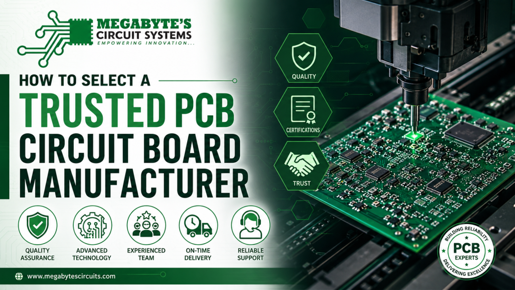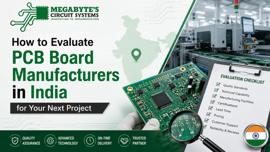
How to Pick the Best PCB Board Manufacturers in India for Your Project
Selecting the right partner from the sea of PCB board manufacturers in India isn’t just about finding the lowest price it’s about finding a team that won’t let your project fail at the finish line. In my 20+ years of hands-on experience at Megabyte Circuit Systems, I’ve seen hundreds of hardware engineers lose weeks of progress because of a poorly etched trace or a delaminated substrate.
In 2026, the Indian electronics landscape has shifted. With the “Make in India” initiative reaching its peak, you now have access to world-class fabrication right here in Ahmedabad and across the country. Whether you are a procurement manager at a Tier-1 industrial house or a startup founder building an IoT wearable, this guide will help you filter through the noise and identify the manufacturers that actually deliver on their promises of quality and lead time.
What Sets Leading PCB Board Manufacturers in India Apart?
Not all fabrication houses are created equal. When we talk about “top-tier” manufacturers, we aren’t just looking at the size of their factory. We are looking at their process control. A top manufacturer treats a Single Layer PCB with the same precision as a 12-layer high-density interconnect (HDI) board.
The best players in the industry differentiate themselves through:
- IPC Class Adherence: Most local shops claim “high quality,” but the leaders strictly follow IPC-A-600 (Acceptability of Printed Boards) and IPC-6012.
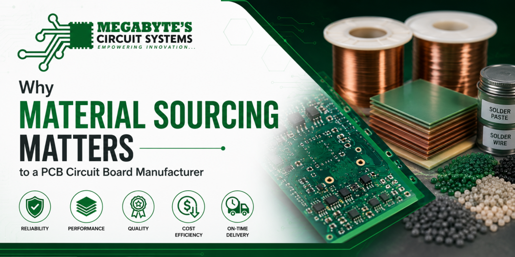
- Material Transparency: They don’t swap out high-grade FR4 for inferior “no-name” laminates to save a few rupees.
- DFM Support: A true partner will catch a clearance issue in your Gerber files before the copper is even etched.
Quick Technical Summary:
Leading manufacturers distinguish themselves by strictly adhering to IPC Class 2 or Class 3 standards and providing comprehensive Design for Manufacturing (DFM) feedback. They utilize automated optical inspection (AOI) and flying probe testing to ensure 0% defect rates before shipping.
Top 10 PCB Board Manufacturers in India for 2026 (Expert Insight)
While the “best” manufacturer depends on your specific volume and complexity, these names consistently lead the market in 2026. I’ve categorized them based on their primary strengths from high-volume giants to specialized quick-turn prototype experts like us.
Manufacturer | Primary Specialization | Best For | Location |
Megabyte Circuit Systems | Quick-Turn & Multilayer | Prototyping & Mid-Scale Production | Ahmedabad |
AT&S India | High-End HDI & Med-Tech | Global Scale / High Complexity | Nanjangud |
Ascent Circuits | Industrial & Automotive | Massive Volume Production | Hosur |
Circuit Systems India (CSIL) | Multilayer Rigid PCBs | Telecom & Defense | Gandhinagar |
Fine-Line Circuits | Precision Fabrication | High-Reliability / Aerospace | Mumbai |
Shogini Electronics | Single/Double Sided | Rapid Consumer Electronics | Pune |
Epitome Components | Large Volume Single-Sided | Home Appliances & Lighting | Ahmednagar |
Genius Electrical | Power Electronics PCBs | Inverters & UPS Manufacturers | Gandhinagar |
Sahasra Electronics | Integrated EMS | Full-Turnkey Solutions | Noida |
CIPSA TEC | Multilayer Standard | Industrial Controls | Tumkur |
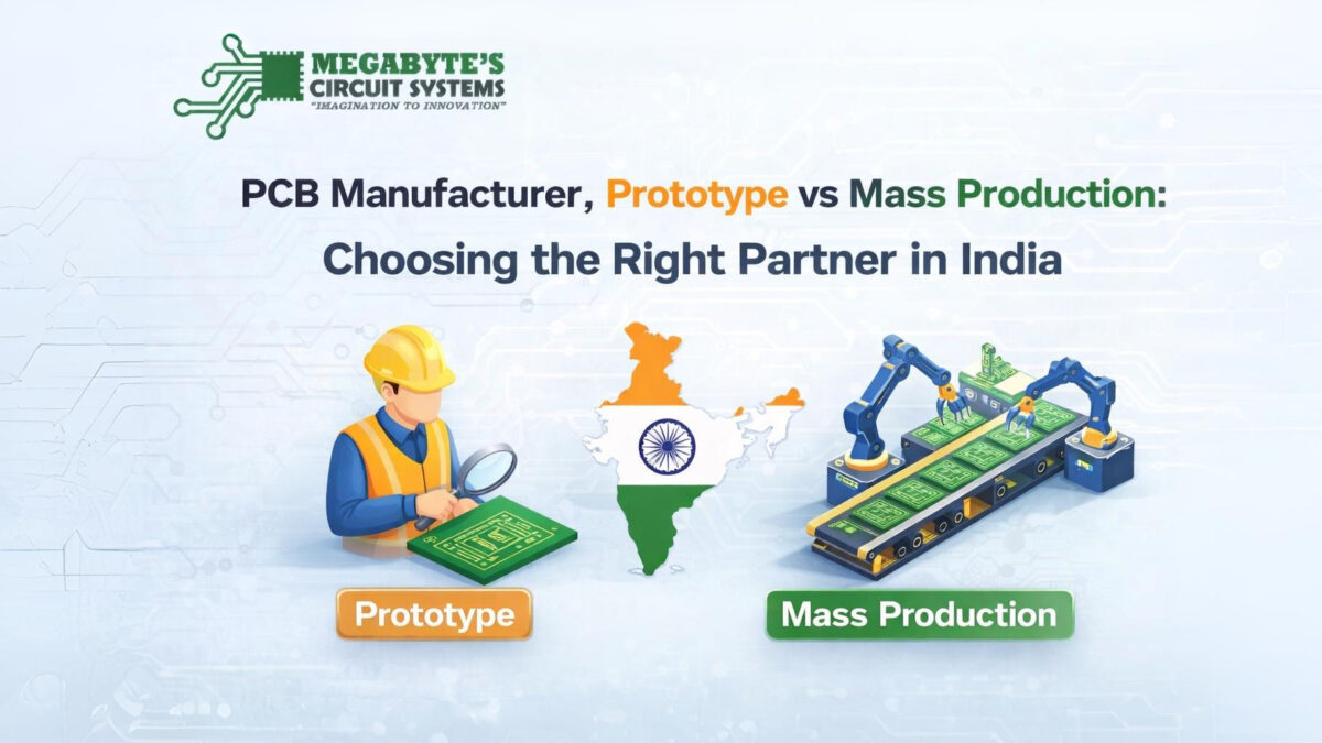
One thing I always tell my clients is: “Don’t go to a high-volume giant for a 5-unit prototype, and don’t go to a prototype shop for 100,000 units.” Finding that “Goldilocks” zone for your specific batch size is the secret to cost-effective sourcing. For many of our clients in Gujarat, our PCB Manufacturing service provides that perfect middle ground between precision and speed.
5 Questions to Ask PCB Board Manufacturers in India Before Ordering
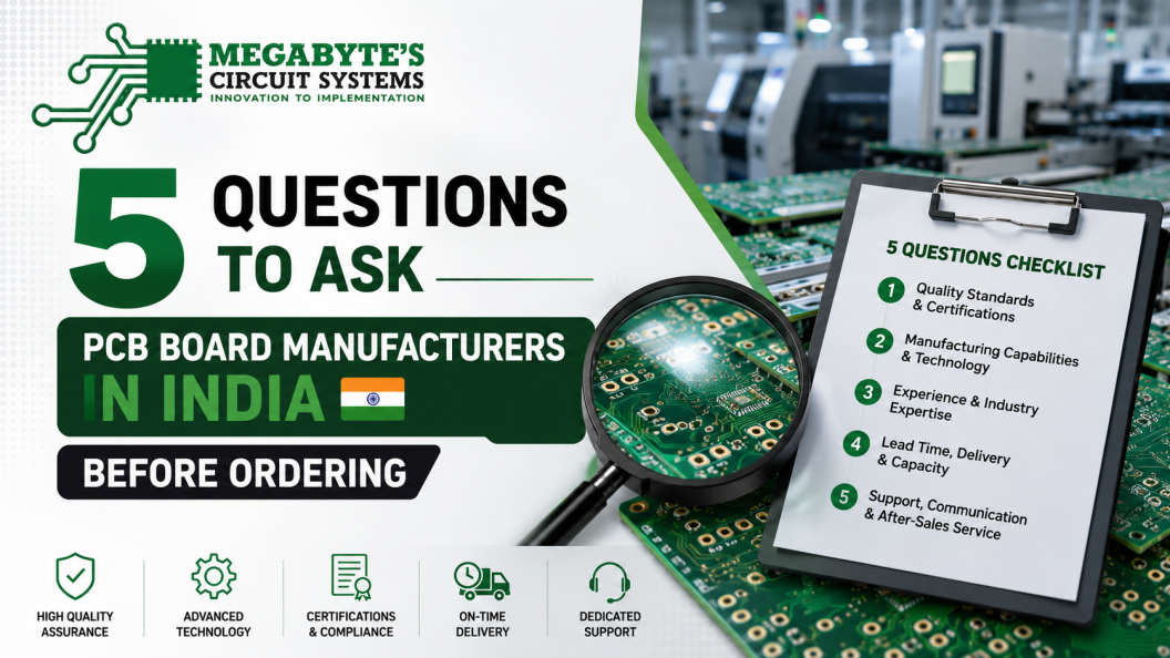
Before you hit “upload” on your Gerber files, I recommend picking up the phone or sending a quick email with these five technical questions. Their answers will tell you more than any brochure ever could.
1. "What is your standard aspect ratio for plated through-holes (PTH)?"
If they can’t handle an aspect ratio of at least 8:1 or 10:1, they may struggle with complex Multilayer PCB designs.
2. "Do you perform 100% Netlist Testing?"
Some low-cost manufacturers only do “visual inspection.” In 2026, you should insist on an E-test (Flying Probe or Bed-of-Nails) against your original netlist.
3. "What are your minimum trace width and spacing capabilities?"
Standard production is usually 6/6 mil (0.15mm). If your IoT design requires 3/3 mil, you need to know if their imaging equipment (LDI vs. Film) can actually hold those tolerances without shorts.
4. "Which laminate brands do you stock?"
Ask for specific names like Kingboard, Shengyi, or Isola. If they are vague about the material, the thermal reliability of your board is at risk.
5. "Can you provide a DFM report before fabrication?"
A manufacturer that offers a PCB Design Service or a thorough DFM check is worth their weight in gold. They are your last line of defense against “unmanufacturable” designs.
Cost Breakdown from Top PCB Board Manufacturers in India
Costing is rarely a flat rate. At Megabyte Circuit Systems, we use a precise PCB Calculator to help engineers budget. However, understanding the “why” behind the price helps you optimize.
- Layer Count: Moving from a Double Layer PCB to 4 layers typically increases the price by 60-80% due to the lamination and extra drilling processes.
- Surface Finish: Lead-free HASL is the “standard” in India, but if you need ENIG (Electroless Nickel Immersion Gold) for fine-pitch components, expect a 10-20% price jump.
- Copper Weight: Standard is 1oz (35μm). If you’re designing for high power and need 2oz or 3oz, the cost of raw material and etching time increases significantly.
Quick Technical Summary:
PCB costs in India are primarily driven by layer count, base material thickness, and surface finish (ENIG vs. HASL). To optimize costs, stick
to standard FR4 materials and 6/6 mil design rules whenever possible.
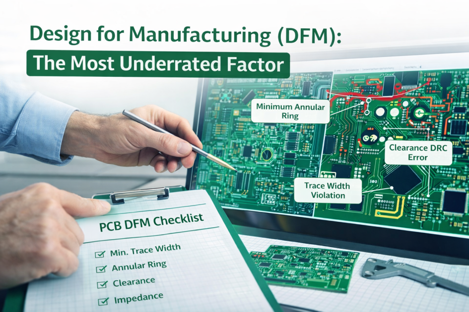
Engineering Checklist: Design for Manufacturing (DFM) for the Indian Market
We see this issue very often: a design looks perfect on the screen but fails on the factory floor. To ensure your boards are manufactured smoothly at any of the top PCB board manufacturers in India, follow this checklist:
- Drill to Copper Clearance: Ensure at least 8-10 mils of clearance between the hole wall and the nearest copper trace to prevent shorts during drilling.
- Solder Mask Expansion: Set a 2-3 mil expansion around pads. If it’s zero, you’ll get mask-on-pad issues that make PCB Assembly service a nightmare.
- Annular Rings: For a 0.3mm drill, ensure your pad is at least 0.6mm. Small annular rings lead to “breakouts” during the plating process.
- Silkscreen Legibility: Keep text height at 30 mils and stroke width at 6 mils. Anything smaller often becomes a blurry mess after the curtain coating process.
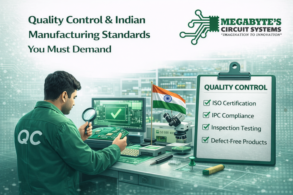
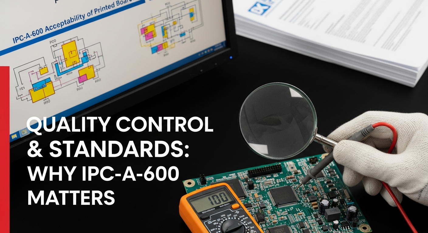
Quality Control Standards in 2026
When evaluating PCB board manufacturers in India, look for the “Big Three” certifications:
- ISO 9001:2015: Ensures a consistent quality management system.
- UL Certification: Essential if you plan to export your product to the US or European markets.
- IPC-A-600 Compliance: The global “bible” for what a good PCB should look like.
At Megabyte, we integrate these standards into our PCB Developing Services. We don’t just “make” the board; we validate it using Cross-section analysis and Micro-sectioning when required for high-reliability industrial clients.
FAQs about PCB Board Manufacturers in India
1. What is the typical lead time for PCB prototyping in India?
For standard double-sided boards, most top manufacturers offer a “Quick-Turn” service of 2 to 5 days. For complex multilayer boards, expect 7 to 10 working days.
2. Can Indian manufacturers handle High-Density Interconnect (HDI) boards?
Yes, but the list of capable vendors shrinks. Only about the top 10-15% of manufacturers in India have the laser drilling and vacuum lamination equipment required for reliable HDI/Blind-Buried via production.
3. Is it cheaper to source PCBs from China or India in 2026?
For very high volumes (10,000+), China remains slightly cheaper. However, for prototypes and mid-scale production, Indian manufacturers are now highly competitive, especially when you factor in 2026 shipping costs, import duties, and the ease of local technical support.
4. What files do I need to provide for a quote?
You should provide your Gerber Files (RS-274X or X2 format), a NC Drill file, and a “ReadMe” text file specifying the board thickness, copper weight, and solder mask color.
5. How do I verify if a manufacturer is truly "Quality Certified"?
Don’t just take their word for it. Ask for a copy of their latest ISO or UL certificate and check the expiry date. Real experts won’t mind sharing their credentials.
Conclusion: Partner with a Manufacturer Who Understands Your Vision
Choosing from the many PCB board manufacturers in India is a decision that impacts your product’s reliability and your company’s reputation. While the “Top 10” list gives you a great starting point, the best manufacturer is the one that acts as an extension of your own engineering team.
At Megabyte Circuit Systems, we’ve built our reputation over two decades by being that partner. Whether you’re in the heart of Ahmedabad or anywhere across India, we make it easy to transition from a schematic to a high-quality physical board.
Ready to bring your design to life?
Upload your Gerber files here for an instant quote, or reach out to our senior consulting team to discuss your custom project requirements. Let’s build something exceptional together.