Categories
PCB Guide

PCB Cost Optimization: How to Use a PCB Cost Calculator Effectively

PCB Cost Optimization: How to Use a PCB Cost Calculator Effectively

In the fast-paced world of electronics, managing production costs is a critical challenge for startups, hobbyists, and established companies alike. Printed circuit boards (PCBs) are the backbone of modern devices, from smartphones to medical equipment, and their production costs can significantly impact a project’s budget. A PCB cost calculator is a powerful tool that helps engineers and businesses estimate expenses, optimize designs, and make informed decisions without compromising quality. By understanding the factors that drive PCB costs and leveraging online tools, you can save money while ensuring high-performance boards.

This guide explores how to use a PCB cost calculator effectively, diving into key cost drivers like board size, layer count, material selection, and order quantity. We’ll provide a step-by-step process, practical tips for startups, and real-world examples to illustrate cost-saving strategies. Whether you’re designing a prototype or scaling production, mastering PCB cost optimization can give you a competitive edge.

Why PCB Cost Optimization Matters

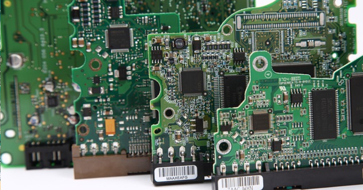
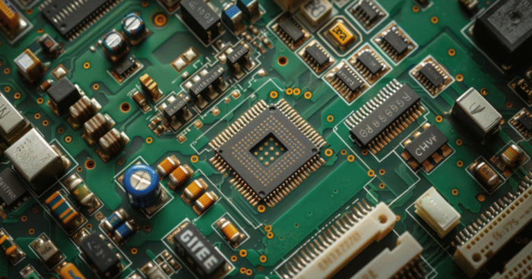
PCBs vary widely in complexity and cost, from simple single-layer boards for hobbyist projects to intricate multilayer designs for aerospace applications. Unoptimized designs can lead to unnecessary expenses, such as oversized boards or excessive layer counts, which inflate production costs. For startups with tight budgets or hobbyists working on personal projects, these costs can be a barrier to innovation. Even large companies benefit from cost optimization to improve margins and stay competitive.

A PCB cost calculator simplifies this process by providing instant cost estimates based on design parameters. For example, a Bangalore-based IoT startup used a cost calculator to reduce their prototype costs by 25% by switching from a 4-layer to a 2-layer PCB without sacrificing functionality. By understanding cost drivers and using these tools, you can make data-driven decisions that balance quality and budget.

Key Factors Influencing PCB Costs

Key Factors Influencing PCB Costs

To optimize PCB costs, you need to understand the primary factors that influence pricing. Below, we explore the most significant cost drivers and how they impact your budget.

Board Size

The physical dimensions of a PCB directly affect material and manufacturing costs. Larger boards require more raw materials (e.g., FR-4 substrate, copper) and take up more space on production panels, increasing costs. For instance, a 10×10 cm board may cost $20 for a prototype, while a 20×20 cm board could cost $40 due to doubled material usage.

Layer Count

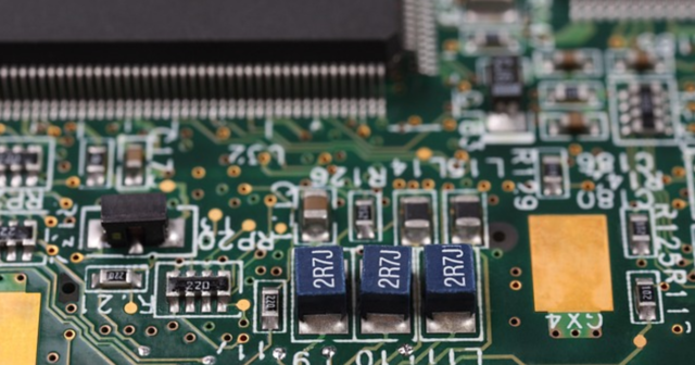
The number of layers in a PCB—ranging from single-layer to multilayer designs—has a significant impact on cost. Single-layer boards are the cheapest, often costing $10–$30 for prototypes, while multilayer boards (4+ layers) can range from $50–$200 due to complex manufacturing processes. Each additional layer increases material, labor, and testing costs.

Material Selection

The choice of substrate material affects both cost and performance. FR-4, a standard fiberglass material, is cost-effective for most applications, costing around $0.05/cm². High-performance materials like Rogers or ceramic substrates, used for high-frequency designs, can cost 2–5 times more. Selecting the right material for your application is crucial for cost optimization.

Order Quantity

PCB manufacturing follows economies of scale. Prototypes (1–10 boards) are expensive per unit due to setup costs, while larger orders (100+ boards) reduce the cost per board. For example, a single prototype might cost $50, but ordering 100 units could drop the price to $5 per board.
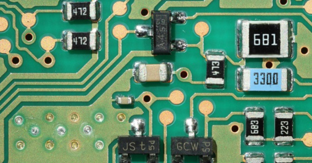
Additional Features

Features like surface finish (e.g., ENIG vs. HASL), via types (e.g., blind or buried vias), and special requirements (e.g., impedance control) add to costs. For instance, ENIG surface finish can add $10–$20 per board compared to HASL, but it’s necessary for high-reliability applications.

How to Use a PCB Cost Calculator: Step-by-Step Guide

A PCB cost calculator is a user-friendly tool that estimates production costs based on your design specifications. Here’s a step-by-step guide to using one effectively.

Step 1: Gather Your Design Specifications

Before using a calculator, collect key details about your PCB:

  • Dimensions: Measure the length and width (e.g., 10×15 cm).
  • Layer Count: Decide on single-layer, double-sided, or multilayer (e.g., 2, 4, or 6 layers).
  • Material: Specify the substrate (e.g., FR-4, Rogers) and copper thickness (e.g., 1 oz/ft²).
  • Quantity: Determine how many boards you need (e.g., 5 for prototyping, 100 for production).
  • Special Requirements: Note any extras like surface finish, via types, or expedited delivery.

Having these details ready ensures accurate cost estimates.

Step 2: Choose a Reliable PCB Cost Calculator

Select a reputable online PCB calculator from manufacturers or platforms like:

  • PCBShopper: Compares quotes from multiple vendors.
  • PCBWay Calculator: Offers detailed cost breakdowns for prototypes and production.
  • OshPark Cost Tool: Ideal for small-batch, high-quality PCBs.

These tools are user-friendly and provide instant quotes based on your inputs.

Step 3: Input Your Specifications

Enter your design details into the calculator. For example:

  • Board size: 10×10 cm
  • Layers: 2
  • Material: FR-4
  • Quantity: 10
  • Surface finish: HASL
  • Turnaround time: Standard (5–7 days)

The calculator will generate an estimated cost, such as $35 for 10 boards, and highlight cost drivers like layer count or expedited shipping.

Step 4: Analyze and Adjust Your Design

Review the cost breakdown provided by the calculator. If the price exceeds your budget, consider adjustments like:

  • Reducing board size by optimizing component placement.
  • Lowering layer count if performance allows (e.g., 4 to 2 layers).
  • Choosing a cheaper surface finish (e.g., HASL instead of ENIG).
  • Increasing order quantity to leverage economies of scale.

For instance, a startup reduced costs by 20% by shrinking their board from 15×15 cm to 12×12 cm after using a cost calculator.

Step 5: Request a Quote and Prototype

Once satisfied with the estimate, submit your design files (e.g., Gerber files) to the manufacturer for a formal quote. Order a small batch of prototypes to test your design before committing to full production.

Tips for Startups to Balance Quality and Budget

Startups often face the challenge of delivering high-quality PCBs on limited budgets. Here are practical strategies to optimize costs without compromising performance:

Optimize Design for Manufacturability

Design for manufacturability (DFM) ensures your PCB is easy and cost-effective to produce. Use standard board sizes (e.g., 10×10 cm) to maximize panel utilization, reducing waste. Avoid unnecessary features like blind vias unless critical for performance. A Chennai-based startup saved 15% on prototype costs by adhering to DFM guidelines provided by their manufacturer.

Choose Cost-Effective Materials

For most applications, FR-4 is sufficient and affordable. Reserve high-cost materials like Rogers for high-frequency or high-reliability designs. Consult with your manufacturer to select materials that meet performance needs without breaking the bank.

Start with Small Batches

Order a small number of prototypes (5–10 boards) to test your design. This minimizes upfront costs and allows you to identify issues before scaling. A Delhi-based IoT company saved $500 by testing a 5-board batch before ordering 100 units.

Leverage Local Manufacturers in India

India’s PCB industry offers competitive pricing and quick turnaround. Manufacturers in cities like Bangalore, Hyderabad, and Ahmedabad provide high-quality prototypes at 30–50% lower costs than Western vendors. For example, a Hyderabad startup reduced prototype costs by 40% by partnering with a local fabricator.

Use Free Design Tools

Free software like KiCad or EasyEDA can reduce design costs compared to paid tools like Altium. These tools include built-in PCB design calculators to estimate trace widths and power requirements, helping you optimize costs early in the design phase.

Real-World Example: Startup Success with Cost Optimization

A Bangalore-based startup developing a smart home sensor faced budget constraints during prototyping. Initially, their 4-layer, 15×15 cm PCB design cost $120 for 5 boards. By using a PCB cost calculator, they identified two cost-saving opportunities:

  • Reducing the board size to 12×12 cm, saving 10% on materials.
  • Switching from a 4-layer to a 2-layer design after verifying that signal integrity was unaffected, cutting costs by 15%.

The revised design cost $90 for 5 boards, saving 25% while maintaining performance. After successful testing, they scaled to 200 units, further reducing the per-board cost to $8. This example shows how PCB cost calculators empower startups to make informed decisions.

Common Cost Optimization Mistakes to Avoid

Common Cost Optimization Mistakes to Avoid
  • Over-Designing Layers: Using more layers than necessary increases costs. Always justify multilayer designs with performance needs.
  • Ignoring DFM Feedback: Manufacturers often provide free DFM checks. Ignoring these can lead to costly reworks.
  • Choosing Cheap Vendors Blindly: Low-cost manufacturers may compromise quality. Select vendors with ISO 9001 certification or positive reviews.
  • Neglecting Prototyping: Skipping prototypes to save money can lead to expensive errors in production.

Downloadable Cost-Saving Checklist

To help you optimize PCB costs, here’s a quick checklist:

  • Use standard board sizes to reduce material waste.
  • Minimize layer count based on performance needs.
  • Select FR-4 for standard applications.
  • Order small prototype batches before scaling.
  • Request DFM feedback from your manufacturer.
  • Use a PCB cost calculator to compare design options.

Download our free PCB cost-saving checklist to streamline your next project.

Why Choose Us for Your PCB Needs?

At Megabyte Circuit System we specialize in PCB board fabrication in India, offering cost-effective solutions for startups and engineers. Our advanced PCB cost calculator provides transparent pricing, and our team helps optimize your design for quality and affordability.

Conclusion

PCB cost optimization is a game-changer for startups and engineers looking to balance quality and budget. By understanding cost drivers like board size, layer count, and material selection, and using tools like PCB cost calculators, you can make informed decisions that save money without compromising performance. The step-by-step guide and tips provided here empower you to streamline your design process, avoid common mistakes.

Whether you’re prototyping a new IoT device or scaling production, optimizing PCB costs is within your reach. Start using a PCB calculator today and take control of your project budget.

Categories
PCB Guide

PCB Power Loss Calculation: A Guide to Efficient Circuit Design

PCB Power Loss Calculation: A Guide to Efficient Circuit Design

In the realm of electronics, designing efficient printed circuit boards (PCBs) is critical for ensuring optimal performance and reliability. One key aspect of this process is understanding and minimizing power loss, which can significantly impact a circuit’s efficiency, thermal performance, and longevity. PCB power loss calculation involves quantifying energy dissipation in a PCB due to resistive, dielectric, and other losses. By mastering these calculations, engineers can create high-performance designs that meet the demands of modern applications, from consumer electronics to aerospace systems.

This guide delves into the technical aspects of PCB power loss calculation, offering a clear explanation of the underlying principles, formulas, and tools like PCB design calculators. We’ll explore best practices for minimizing losses and provide practical insights for engineers aiming to optimize their designs.

Understanding Power Loss in PCBs

Power loss in a PCB occurs when electrical energy is converted into heat or other forms of energy, reducing the efficiency of the circuit. These losses primarily stem from three sources: resistive losses in copper traces, dielectric losses in the PCB substrate, and parasitic losses due to components or layout inefficiencies. Each type of loss affects the performance of high-speed or high-power circuits, such as those in 5G infrastructure, electric vehicles, or medical devices.

Resistive losses, often the most significant, occur due to the resistance of copper traces and vias. Dielectric losses arise from the insulating material’s interaction with high-frequency signals, while parasitic losses result from unintended capacitances or inductances in the layout. By calculating and mitigating these losses, engineers can improve signal integrity, reduce heat generation, and extend the lifespan of the PCB.

Why Power Loss Calculation Matters

Power Loss Calculation Matters

Accurate PCB power loss calculation is essential for several reasons. First, excessive power loss leads to heat buildup, which can degrade components, reduce reliability, and necessitate costly cooling solutions. Second, power loss impacts energy efficiency, a critical factor in battery-powered devices like wearables or IoT modules. Finally, in high-frequency applications, such as telecommunications, power loss can distort signals, leading to data errors or performance degradation.

For example, in a real-world scenario, a startup designing a drone’s control system found that unoptimized trace widths caused 15% higher power loss, reducing flight time. By recalculating and adjusting their PCB design, they improved efficiency and extended battery life by 20%. Such outcomes highlight the importance of precise power loss calculations in achieving efficient circuit designs.

Key Components of PCB Power Loss

To calculate power loss effectively, engineers must focus on the primary contributors: resistive, dielectric, and parasitic losses. Below, we explore each in detail to provide a foundation for accurate calculations.

Resistive Losses in Copper Traces

Resistive losses occur when current flows through copper traces, which have inherent resistance. The power loss due to resistance is governed by Joule’s Law, expressed as:

[ P = I^2 \cdot R ]

Where ( P ) is the power loss (in watts), ( I ) is the current (in amperes), and ( R ) is the resistance (in ohms). The resistance of a trace depends on its material, length, width, and thickness, calculated as:

[ R = \rho \cdot \frac{L}{A} ]

Where ( \rho ) is the resistivity of copper (approximately ( 1.68 \times 10^{-8} , \Omega \cdot m )), ( L ) is the trace length, and ( A ) is the cross-sectional area (width × thickness). For high-current designs, wider and thicker traces reduce resistance and, consequently, power loss.

Dielectric Losses in PCB Substrates

Dielectric losses occur in the insulating material (e.g., FR-4, Rogers) between conductive layers, especially at high frequencies. These losses are quantified using the dissipation factor (Df) and are calculated as:

[ P_d = \pi \cdot f \cdot C \cdot V^2 \cdot \tan \delta ]

Where ( P_d ) is the dielectric power loss, ( f ) is the signal frequency, ( C ) is the capacitance, ( V ) is the voltage, and ( \tan \delta ) is the dissipation factor. Materials with lower dissipation factors, such as Rogers substrates, are preferred for high-frequency applications to minimize dielectric losses.

Parasitic Losses

Parasitic losses arise from unintended capacitances and inductances in the PCB layout, such as those caused by closely spaced traces or vias. These losses are harder to quantify but can be estimated using simulation tools. Proper layout techniques, like maintaining adequate trace spacing and optimizing via placement, help reduce parasitic effects.

Tools for PCB Power Loss Calculation

Manually calculating power loss can be complex, especially for multilayer PCBs with intricate layouts. Fortunately, PCB design calculators and software tools simplify the process by automating calculations and providing actionable insights.

PCB Design Calculators

Online PCB design calculators allow engineers to input parameters like trace width, length, current, and material properties to estimate power loss. Popular tools include:

  • Saturn PCB Toolkit: A free tool for calculating trace resistance, power loss, and thermal effects.
  • Altium Designer’s PDN Analyzer: Simulates power distribution and identifies loss hotspots.
  • KiCad’s Calculator Tools: Offers built-in utilities for trace resistance and via calculations.

These tools provide quick estimates, enabling engineers to iterate designs efficiently. For example, a designer can use the Saturn PCB Toolkit to determine that a 10-mil trace carrying 2A results in 0.5W of power loss, prompting a switch to a wider trace.

Simulation Software

Advanced simulation software, such as ANSYS HFSS or Cadence Sigrity, models power loss in high-frequency or complex PCBs. These tools analyze resistive, dielectric, and parasitic losses across the entire board, offering detailed visualizations of loss distribution. While more expensive, they are invaluable for high-stakes projects like aerospace or telecommunications.

Best Practices for Minimizing Power Loss

Reducing power loss is a critical step in achieving efficient PCB designs. Below are proven strategies to optimize your circuit and minimize energy dissipation.

Optimize Trace Geometry

To reduce resistive losses, design traces with appropriate width and thickness based on current requirements. For high-current paths, use wider traces or increase copper thickness (e.g., 2 oz/ft² instead of 1 oz/ft²). Shortening trace lengths by optimizing component placement also lowers resistance. For example, in a power supply PCB, repositioning a regulator closer to the load reduced trace length by 20%, cutting power loss by 10%.

Select Low-Loss Materials

Choose PCB substrates with low dissipation factors for high-frequency designs. While FR-4 is cost-effective for standard applications, materials like Rogers RO4003C offer lower dielectric losses for RF circuits. Consult with your manufacturer to balance performance and cost. A telecommunications company reported a 15% reduction in signal loss by switching to a low-loss substrate for their 5G base station PCBs.

Implement Power and Ground Planes

In multilayer PCBs, dedicate entire layers to power and ground planes to reduce resistance and improve current distribution. This approach minimizes voltage drops and enhances signal integrity. For instance, a 4-layer PCB with a dedicated ground plane reduced power loss by 12% compared to a 2-layer design in a medical imaging device.

Minimize Parasitic Effects

Careful layout design can reduce parasitic losses. Maintain adequate spacing between high-speed signal traces to prevent crosstalk, and use vias strategically to avoid unnecessary inductance. Simulation tools can help identify parasitic hotspots before fabrication. A case study from an IoT startup showed that optimizing via placement reduced parasitic losses by 8%, improving device reliability.

Use Thermal Management Techniques

Excessive power loss generates heat, which can degrade performance. Incorporate thermal vias, heat sinks, or copper pours to dissipate heat effectively. For high-power designs, consider active cooling solutions like fans. A drone manufacturer used thermal vias in their motor control PCB, reducing operating temperatures by 10°C and extending component life.

Real-World Applications

PCB power loss calculation is critical in various industries. For example:

  • Electric Vehicles: Tesla’s battery management systems use optimized PCBs to minimize power loss, ensuring longer driving ranges.
  • 5G Infrastructure: Nokia’s base stations rely on low-loss PCBs to maintain signal integrity at high frequencies.
  • Medical Devices: Wearable heart monitors use efficient PCB designs to maximize battery life, ensuring continuous operation.

These examples demonstrate how precise power loss calculations lead to better performance and competitive advantages.

How to Get Started with Power Loss Optimization

Get Started with Power Loss Optimization

To integrate power loss calculations into your design process:

  1. Analyze Requirements: Determine current, frequency, and thermal constraints for your PCB.
  2. Use Calculators: Leverage tools like Saturn PCB Toolkit for quick estimates.
  3. Simulate Designs: Use software like Altium or ANSYS for detailed analysis.
  4. Collaborate with Manufacturers: Work with experienced PCB fabricators to validate designs. Get a quote for optimized PCB fabrication.
    1. Test Prototypes: Build and test prototypes to verify power loss predictions.

Why Choose Us for Your PCB Design Needs?

At Megabyte Circuit System, we specialize in designing and fabricating efficient PCBs tailored to your needs. Our team uses advanced PCB design calculators and simulation tools to minimize power loss and ensure high performance. Whether you’re developing a prototype or scaling to production, we’re here to help. Contact us for expert PCB design services.

Conclusion

PCB power loss calculation is a cornerstone of efficient circuit design, enabling engineers to create reliable, high-performance electronics. By understanding resistive, dielectric, and parasitic losses, and using tools like PCB design calculators, you can optimize your designs for minimal energy dissipation. Best practices, such as optimizing trace geometry, selecting low-loss materials, and implementing power planes, further enhance efficiency.

As industries like electric vehicles, 5G, and medical devices demand ever-higher performance, mastering power loss calculation gives you a competitive edge. Start optimizing your PCBs today and unlock the full potential of your designs. Request a quote for PCB fabrication services to partner with us and achieve superior circuit efficiency.

Categories
PCB Guide

Prototype PCB in India: How to Get Started with Your First Board

Prototype PCB in India: How to Get Started with Your First Board

For startups, hobbyists, and engineers, creating a prototype PCB in India is a critical step in turning innovative ideas into functional products. A prototype printed circuit board (PCB) is a preliminary version of a circuit board used to test designs before mass production. With India emerging as a hub for electronics manufacturing, prototyping has become more accessible and cost-effective. Whether you’re designing a smart device, IoT module, or medical equipment, understanding the prototyping process in India can save time, reduce costs, and ensure quality.

This comprehensive guide walks you through the process of creating your first prototype PCB in India, covering local manufacturers, costs, challenges, and a step-by-step approach. By leveraging India’s growing PCB industry, you can bring your vision to life efficiently. Ready to start your prototyping journey? Contact us for expert PCB fabrication services.

Why Choose India for PCB Prototyping?

Choose India for PCB Prototyping

India’s electronics sector is booming, driven by government initiatives like “Make in India” and a skilled workforce. Here’s why PCB board fabrication in India is ideal for prototyping:

  • Cost-Effectiveness: Lower labor and material costs make India a budget-friendly option compared to Western markets.
  • Local Expertise: Cities like Bangalore, Delhi, and Pune host numerous PCB manufacturers with advanced facilities.
  • Quick Turnaround: Proximity to local suppliers ensures faster delivery, often within days for prototypes.
  • Growing Infrastructure: Investments in automation and technology have improved the quality of PCB fabrication in India.

For startups and hobbyists, these advantages make India an attractive destination for prototyping innovative electronics.

Step-by-Step Guide to Creating Your First Prototype PCB in India

Follow this detailed process to develop your first prototype PCB in India, from concept to finished board.

Step 1: Define Your PCB Requirements

Before contacting a manufacturer, clarify your project’s specifications:

  • Board Type: Single-layer, double-sided, or multilayer PCB.
  • Size and Shape: Determine dimensions and any custom shapes.
  • Components: List components (e.g., resistors, ICs) and their placement needs.
  • Performance Needs: Specify signal speed, power requirements, or thermal constraints.
  • Quantity: Decide how many prototype boards you need (typically 1–10 for initial testing).

Tip: Use a checklist to ensure all requirements are documented. This helps manufacturers provide accurate quotes.

Step 2: Design Your PCB

Use PCB design software to create your schematic and layout:

  • Popular Tools: KiCad (free), Altium Designer, or Eagle for professional designs.
  • Key Design Considerations:
    • Ensure proper trace widths for current capacity.
    • Optimize via placement to avoid signal interference.
    • Include test points for debugging.
  • Design Rule Check (DRC): Run DRC to catch errors like overlapping traces or incorrect spacing.

Case Study: A Bangalore-based startup designing an IoT sensor used KiCad to create a 4-layer prototype PCB, reducing design costs by 30% compared to proprietary software.

Step 3: Select a Reliable PCB Manufacturer in India

Choosing the right manufacturer is critical for quality and reliability. Look for:

  • Experience: Manufacturers with a track record in prototype PCB in India.
  • Capabilities: Support for multilayer boards, surface-mount technology (SMT), and quick-turn services.
  • Certifications: ISO 9001 or IPC standards for quality assurance.
  • Customer Reviews: Check testimonials or case studies for credibility.

Top Indian Manufacturers:

  • PCB Power Market (Ahmedabad): Known for quick-turn prototypes and online ordering.
  • CEM Solutions (Bangalore): Specializes in multilayer PCBs for startups.
  • Sion Semiconductors (Hyderabad): Offers end-to-end prototyping and assembly.

Tip: Request quotes from multiple manufacturers to compare pricing and lead times. Get a quote from our trusted PCB fabrication services.

Step 4: Generate and Submit Gerber Files

Gerber files are the industry-standard format for PCB manufacturing. They include:

  • Copper layers
  • Solder mask
  • Silkscreen
  • Drill files

Use your design software to export Gerber files and verify them using a Gerber viewer (e.g., Gerbv). Submit these files to your chosen manufacturer along with a Bill of Materials (BOM) listing all components.

Common Mistake: Incomplete Gerber files can delay production. Double-check that all layers are included.

Step 5: Prototype Fabrication

The manufacturer will fabricate your PCB based on the provided files. The process includes:

  • Material Selection: FR-4 is common for prototypes due to its affordability and durability.
  • Fabrication: Etching copper layers, drilling vias, and applying solder mask.
  • Quality Checks: Automated optical inspection (AOI) to detect defects.

Lead times for PCB board fabrication in India typically range from 3–10 days for prototypes, depending on complexity.

Step 6: Assembly and Component Sourcing

After fabrication, components are mounted on the board:

  • Manual Assembly: Suitable for small batches or complex designs.
  • SMT Assembly: Automated for high precision and speed.
  • Component Sourcing: Manufacturers may source components, or you can provide them. Local distributors like Element14 India offer quick access to parts.

Testimonial: “We partnered with a Delhi-based PCB fabricator for our prototype. Their SMT assembly saved us 40% on production time,” says Anil K., a startup founder.

Step 7: Testing and Validation

Test your prototype to ensure it meets design expectations:

  • Functional Testing: Verify circuit performance using multimeters or oscilloscopes.
  • Environmental Testing: Check for thermal or vibration resistance if needed.
  • Debugging: Identify and fix issues like short circuits or signal noise.

Tip: Order extra prototype boards to test multiple iterations and avoid delays.

Step 8: Iterate and Scale

Based on test results, refine your design and order additional prototypes if needed. Once satisfied, transition to small-batch or full-scale production with the same manufacturer to maintain consistency.

Costs of Prototype PCB in India

Costs of Prototype PCB in India

The cost of prototype PCB in India depends on several factors:

  • Board Complexity: Single-layer boards cost $10–$50, while multilayer boards range from $50–$200 for prototypes.
  • Quantity: Small batches (1–5 boards) are pricier per unit than larger orders.
  • Turnaround Time: Express services (24–48 hours) increase costs by 20–50%.
  • Assembly: SMT assembly adds $20–$100, depending on component count.

Example: A 2-layer, 10×10 cm prototype with SMT assembly typically costs $30–$80 in India, compared to $100–$200 in the US.

Tip: Use a PCB cost calculator to estimate expenses and optimize your design for cost savings. Try our PCB cost calculator today.

Challenges in PCB Prototyping in India

While India offers many advantages, prototyping can face challenges:

  • Quality Variability: Some low-cost manufacturers may compromise on quality. Solution: Choose certified vendors with positive reviews.
  • Supply Chain Delays: Component shortages can delay assembly. Solution: Partner with manufacturers who offer in-house sourcing.
  • Design Errors: Incorrect Gerber files or poor design can lead to faulty boards. Solution: Use DRC and consult with manufacturers during the design phase.
  • Communication Gaps: Misunderstandings with manufacturers can cause delays. Solution: Provide clear specifications and maintain regular contact.

Case Study: A Pune-based hobbyist faced delays due to incomplete Gerber files. By working closely with their manufacturer’s design team, they resolved the issue and received their prototype in 5 days.

Tips for Successful PCB Prototyping in India

  1. Start Small: Begin with a simple design to test the prototyping process.
  2. Leverage Local Expertise: Collaborate with manufacturers for design feedback.
  3. Plan for Iterations: Budget for multiple prototype rounds to perfect your design.
  4. Explore Online Platforms: Websites like PCB Power Market allow easy ordering and tracking.
  5. Stay Updated: Follow industry trends, such as eco-friendly PCBs or automation, to stay competitive.

Why Choose Us for Your Prototype PCB Needs?

At [Your Company Name], we specialize in PCB board fabrication in India, offering quick-turn prototypes tailored to startups and hobbyists. Our ISO-certified facilities and experienced team ensure high-quality boards at competitive prices. Whether you need a single-layer prototype or a complex multilayer design, we’re here to help. Request a quote for your prototype PCB today.

Conclusion

Creating a prototype PCB in India is an exciting opportunity for startups and hobbyists to innovate affordably. By following the step-by-step process defining requirements, designing, selecting a manufacturer, and testing you can develop a high-quality prototype that sets the stage for successful production. India’s cost-effective manufacturing, skilled workforce, and growing infrastructure make it an ideal destination for PCB prototyping.

Overcome challenges like quality variability and supply chain delays by partnering with reputable manufacturers and leveraging tools like PCB design software and cost calculators. Ready to bring your idea to life? Contact us for expert PCB prototyping services and start building your future today.

Categories
PCB Guide

Multi-Layer Boards: Applications and Benefits in High-Tech Industries

Multi-Layer Boards: Applications and Benefits in High-Tech Industries

In the rapidly evolving world of electronics, multi-layer boards (also known as multilayer PCBs) have become the backbone of high-performance devices. Unlike single-layer or double-sided printed circuit boards, multilayer PCBs consist of three or more conductive layers separated by insulating materials. These boards are designed to handle complex circuits, offering superior functionality, reliability, and compactness. As industries like aerospace, medical, and telecommunications push the boundaries of technology, multilayer PCBs have emerged as the preferred choice for meeting their demanding requirements.

This blog explores the applications of multilayer PCBs in high-tech industries, their key benefits, and why they are essential for modern electronics. Whether you’re an engineer, a product developer, or a business looking to innovate, understanding the power of multilayer PCBs can help you make informed decisions for your next project. Ready to optimize your circuit design? Contact us for expert PCB fabrication services.

What Are Multi-Layer Boards?

A multilayer PCB is a printed circuit board with multiple layers of copper traces, typically ranging from 4 to 12 layers or more, stacked and bonded together. These layers are interconnected using vias (small conductive holes) to route signals and power efficiently. The complexity of multilayer PCBs allows them to support high-density circuits, making them ideal for advanced applications where space, performance, and reliability are critical.

Unlike single-layer PCBs, which are limited to simple electronics like calculators, or double-sided PCBs used in basic consumer devices, multilayer PCBs excel in scenarios requiring intricate designs, high-speed signals, and robust power management. Their ability to pack more functionality into a smaller footprint has made them indispensable in high-tech industries.

Applications of Multi-Layer Boards in High-Tech Industries

Multi-Layer Boards in High-Tech Industries

Multilayer PCBs are at the heart of cutting-edge technologies across various sectors. Below, we explore their key applications in aerospace, medical, and telecommunications, with real-world examples to illustrate their impact.

1. Aerospace Industry

The aerospace sector demands electronics that are lightweight, reliable, and capable of operating in extreme conditions. Multilayer PCBs meet these needs by enabling compact, high-performance circuits for applications such as:

  • Avionics Systems: Flight control systems, radar, and navigation equipment rely on multilayer PCBs to process complex signals with minimal latency. For example, modern aircraft like the Boeing 787 use multilayer PCBs to integrate sensors, communication systems, and control units into a single, lightweight board.
  • Satellites: Space applications require PCBs that can withstand radiation and temperature fluctuations. Multilayer PCBs provide the density and shielding needed for satellite communication systems, such as those used in SpaceX’s Starlink satellites.
  • Drones: Unmanned aerial vehicles (UAVs) use multilayer PCBs to integrate GPS, cameras, and control systems into compact designs, ensuring portability and functionality.

Why Multilayer PCBs? Their ability to handle high-speed signals and reduce electromagnetic interference (EMI) ensures reliable performance in mission-critical aerospace applications.

2. Medical Industry

In the medical field, precision and reliability are non-negotiable. Multilayer PCBs power life-saving devices by supporting complex circuitry in compact forms. Key applications include:

  • Medical Imaging: Devices like MRI and CT scanners use multilayer PCBs to process high-resolution signals and manage multiple data streams. For instance, GE Healthcare’s imaging systems rely on multilayer boards for real-time data processing.
  • Wearable Devices: Smart health monitors, such as heart rate trackers and insulin pumps, use multilayer PCBs to integrate sensors, processors, and wireless communication into small, wearable formats.
  • Surgical Equipment: Robotic surgery systems, like those from Intuitive Surgical, depend on multilayer PCBs for precise control and real-time feedback during operations.

Why Multilayer PCBs? Their high density allows for miniaturization, while their reliability ensures consistent performance in critical medical applications.

3. Telecommunications Industry

The telecommunications sector drives connectivity through devices that require high-speed data transfer and robust signal integrity. Multilayer PCBs are critical in:

  • 5G Infrastructure: Base stations and routers for 5G networks use multilayer PCBs to handle high-frequency signals and complex data processing. Companies like Nokia and Huawei rely on these boards for their 5G equipment.
  • Smartphones: Modern smartphones, such as the iPhone or Samsung Galaxy, use multilayer PCBs to pack processors, memory, and wireless modules into slim designs.
  • IoT Devices: Internet of Things (IoT) devices, like smart home hubs, use multilayer PCBs to integrate multiple communication protocols (Wi-Fi, Bluetooth) in compact forms.

Why Multilayer PCBs? They support high-speed signal transmission and reduce signal loss, making them ideal for the demands of modern telecommunications.

How to Use a PCB Calculator for Cost Management

A PCB Calculator is an intuitive tool that automates cost estimation, eliminating the need for manual calculations or specialized software. Here’s how it functions at Megabytes Circuit Systems:

  1. Input Design Details
    Enter your board’s dimensions, layer count, and copper thickness. For instance, a double-sided board for a consumer gadget differs from a multilayer design for medical equipment. The tool allows you to explore various configurations to understand their cost implications.
  2. Select Materials and Finishes
    Choose materials like FR4 for general use, polyimide for flexibility, or Rogers for high-frequency needs. Pick surface treatments, such as HASL for affordability or ENIG for reliability. The calculator compares options to align with your budget and performance goals.
  3. Plan Trace Width and Impedance
    Ensure your design supports current loads without issues by calculating trace widths, critical for preventing overheating or signal loss. Impedance planning is essential for high-speed applications, like telecommunications or automotive systems, to maintain signal quality.
  4. Receive Instant Cost Estimates
    Get a detailed breakdown of manufacturing, assembly, and shipping expenses. The tool is optimized for online ordering in India, offering clarity on logistics and delivery timelines, including expedited options for urgent projects.
  5. Adjust for Budget Optimization
    Modify parameters like board size, layer count, or material to reduce costs while maintaining quality. For example, downsizing the board or opting for HASL can yield significant savings.

Benefits of Multi-Layer Boards

The widespread adoption of multilayer PCBs in high-tech industries is driven by their unique advantages. Below are the key benefits that make them the go-to choice for complex electronics.

1. Compact Design and Space Efficiency

Multilayer PCBs allow designers to stack multiple layers of circuitry, reducing the board’s footprint. This is critical for applications like smartphones and medical wearables, where space is limited. By integrating more functionality into a smaller area, multilayer PCBs enable sleek, portable devices without sacrificing performance.

2. Enhanced Signal Integrity

High-speed applications, such as 5G networks and avionics, require minimal signal loss and interference. Multilayer PCBs use dedicated ground and power planes to reduce EMI and crosstalk, ensuring clean signal transmission. This is especially important in telecommunications and aerospace, where data accuracy is paramount.

3. Increased Reliability

The layered structure of multilayer PCBs provides better thermal management and mechanical stability. By distributing heat and stress across multiple layers, these boards are less prone to failure, making them ideal for harsh environments like space or medical operating rooms.

4. Greater Design Flexibility

With multiple layers, designers can separate power, ground, and signal planes, optimizing the board for specific functions. This flexibility allows multilayer PCBs to support complex circuits, such as those in IoT devices or advanced medical equipment, without compromising performance.

5. Cost-Effective for Complex Applications

While multilayer PCBs may have higher upfront costs than single-layer boards, their ability to integrate multiple functions into one board reduces the need for additional components and connectors. This makes them cost-effective for high-tech applications where performance outweighs initial investment.

Challenges of Multi-Layer Boards and Solutions

Despite their advantages, multilayer PCBs come with challenges. Manufacturing is more complex, requiring advanced equipment and skilled technicians. Design errors, such as improper via placement, can lead to signal issues or board failure. Additionally, testing and debugging multilayer PCBs can be time-consuming due to their layered structure.

Solutions:

  • Use advanced design software like Altium or KiCad to simulate and verify designs.
  • Partner with experienced manufacturers who specialize in multilayer PCB production.
  • Conduct thorough testing, such as automated optical inspection (AOI) and X-ray analysis, to ensure quality.

Real-World Examples of Multi-Layer Boards in Action

To illustrate the impact of multilayer PCBs, consider these examples:

  • Tesla’s Electric Vehicles: Tesla’s advanced driver-assistance systems (ADAS) rely on multilayer PCBs to process data from cameras, radar, and sensors in real time, enabling features like Autopilot.
  • Fitbit Wearables: Fitbit devices use multilayer PCBs to integrate heart rate sensors, Bluetooth modules, and displays into compact, wrist-worn designs.
  • Ericsson’s 5G Base Stations: These stations use multilayer PCBs to manage high-frequency signals, ensuring seamless connectivity for 5G networks.

These examples highlight how multilayer PCBs drive innovation across industries, enabling smaller, smarter, and more reliable devices.

Optimizing Your Project with Multi-Layer Boards

Headquartered in Ahmedabad, Gujarat, Megabytes Circuit Systems is a trusted PCB manufacturer in India, recognized for quality and innovation. Our ISO-certified facility produces high-performance boards with rigorous testing for functionality, durability, and compliance. Key advantages include:

  • Skilled Team: Experienced engineers and technicians ensure every board meets global standards.
  • End-to-End Services: From design and prototyping to assembly and testing, we manage every stage.
  • Local and National Support: Personalized assistance for Gujarat clients and efficient online ordering for customers across India.
  • Quality Commitment: Comprehensive inspections, including automated optical inspection (AOI) and X-ray testing, guarantee dependable results.

Whether you’re managing circuit board expenses or seeking a custom solution, our team is dedicated to your project’s success.

Online PCB trace width and cost estimation tool interface screenshot

To leverage the benefits of multilayer PCBs, consider these best practices:

  1. Define Requirements Early: Specify the number of layers, signal speed, and thermal needs during the design phase.
  2. Choose the Right Manufacturer: Work with a reputable PCB fabricator with expertise in multilayer boards. Get a quote for multilayer PCB fabrication today.
  3. Test Rigorously: Use prototyping to identify and fix issues before full-scale production.
  4. Stay Updated on Trends: Explore advancements like flexible multilayer PCBs or eco-friendly materials to stay competitive.

Why Choose Us for Your Multilayer PCB Needs?

At [Your Company Name], we specialize in multilayer PCB production tailored to high-tech industries. Our state-of-the-art facilities and experienced team ensure high-quality boards that meet your specifications. Whether you’re developing aerospace avionics, medical devices, or 5G infrastructure, we’ve got you covered. Contact us now to start your project.

Conclusion

Multi-layer boards are revolutionizing high-tech industries by enabling compact, reliable, and high-performance electronics. From aerospace avionics to medical imaging and 5G telecommunications, multilayer PCBs are the foundation of modern innovation. Their benefits compact design, enhanced signal integrity, and greater reliability make them the preferred choice for complex circuits.

As technology continues to advance, the demand for multilayer PCBs will only grow. By understanding their applications and advantages, you can make informed decisions to optimize your projects. Ready to bring your ideas to life? Request a quote for multilayer PCB fabrication and partner with us to power your next innovation.

Categories
PCB Guide

Understanding PCB Costs in India with a PCB Calculator

Understanding PCB Costs in India with a PCB Calculator

A PCB Calculator helps you navigate circuit board expenses in India by offering instant cost estimates tailored to your design specifications, such as size, materials, and order volume. Enter your design details, choose materials, plan trace widths, receive quotes, and adjust for budget. At Megabytes Circuit Systems, our calculator simplifies design cost management for engineers, startups, and hobbyists. This article explores factors influencing costs, how to use our tool effectively, and practical tips to save money, with insights for users in Ahmedabad and across India.

The Importance of Managing Circuit Board Expenses

Producing a Printed Circuit Board (PCB) involves several cost factors that can challenge budget planning for engineers, startups, and hobbyists. Understanding these expenses ensures projects remain financially viable, especially in a competitive market like India. A PCB Calculator streamlines this process by providing real-time, customized cost estimates, enabling informed decisions without complex manual calculations.

At Megabytes Circuit Systems, located in Ahmedabad, Gujarat, our calculator is designed to address the needs of Indian users, offering clarity on expenses whether you’re in Gujarat or ordering online nationwide. From consumer electronics to medical equipment, this tool supports efficient design cost management, helping you create high-quality PCBs affordably.

Key Factors Influencing PCB Costs in India

Several elements shape the expenses of manufacturing a PCB in India, each impacting your project’s budget:

  • Size and Layer Complexity: Larger boards or those with multiple layers require more materials and intricate production processes, driving up costs. Single-layer boards are typically more economical for basic applications.
  • Material Choices: Standard materials like FR4 are budget-friendly, while specialized options like Rogers or Aluminum, suited for high-frequency or thermal applications, come at a premium.
  • Surface Treatments: Finishes such as Hot Air Solder Leveling (HASL) are cost-effective, whereas Electroless Nickel Immersion Gold (ENIG) or Organic Solderability Preservative (OSP) enhance durability but increase expenses.
  • Order Volume: Larger orders benefit from economies of scale, reducing the cost per unit, while prototypes or small batches often incur higher per-unit costs due to setup requirements.
  • Regional Differences: Costs can vary by location, influenced by local manufacturing hubs. For instance, expenses in Ahmedabad may differ from those in Bangalore or Mumbai.
  • Additional Processes: Services like assembly, expedited production, or advanced testing (e.g., X-ray inspection) add to the total cost.

Our calculator considers these factors, delivering a transparent cost overview tailored to your project, whether you’re sourcing locally or ordering online.

How to Use a PCB Calculator for Cost Management

A PCB Calculator is an intuitive tool that automates cost estimation, eliminating the need for manual calculations or specialized software. Here’s how it functions at Megabytes Circuit Systems:

  1. Input Design Details
    Enter your board’s dimensions, layer count, and copper thickness. For instance, a double-sided board for a consumer gadget differs from a multilayer design for medical equipment. The tool allows you to explore various configurations to understand their cost implications.
  2. Select Materials and Finishes
    Choose materials like FR4 for general use, polyimide for flexibility, or Rogers for high-frequency needs. Pick surface treatments, such as HASL for affordability or ENIG for reliability. The calculator compares options to align with your budget and performance goals.
  3. Plan Trace Width and Impedance
    Ensure your design supports current loads without issues by calculating trace widths, critical for preventing overheating or signal loss. Impedance planning is essential for high-speed applications, like telecommunications or automotive systems, to maintain signal quality.
  4. Receive Instant Cost Estimates
    Get a detailed breakdown of manufacturing, assembly, and shipping expenses. The tool is optimized for online ordering in India, offering clarity on logistics and delivery timelines, including expedited options for urgent projects.
  5. Adjust for Budget Optimization
    Modify parameters like board size, layer count, or material to reduce costs while maintaining quality. For example, downsizing the board or opting for HASL can yield significant savings.

Advantages of Megabytes’ PCB Calculator

Our calculator at Megabytes Circuit Systems is crafted for Indian users, offering distinct benefits:

  • Regional Cost Insights: Provides accurate estimates reflecting expenses in Ahmedabad and other Indian cities.
  • Flexible Order Sizes: Supports small batches or single prototypes, ideal for startups and hobbyists.
  • Rapid Processing: Delivers quotes and prototypes swiftly, with expedited delivery from our Ahmedabad facility.
  • Wide-Ranging Tools: Includes features like impedance calculation, layer stack-up planning, and trace width estimation, addressing diverse design needs.
  • Accessible Design: Easy-to-use interface for professionals and beginners, available on both desktop and mobile.

This tool simplifies design cost management, making it a valuable resource for projects of any scale, from initial prototypes to large production runs.

Practical Tips to Lower PCB Expenses

Practical Tips to Lower PCB Expenses

To optimize your budget using the PCB Calculator, consider these strategies:

  • Start with Prototypes: Test a small batch to catch design flaws early, avoiding expensive revisions. Prototyping validates functionality before scaling up.
  • Reduce Layer Count: Opt for single or double-sided boards for simpler projects to minimize material and production costs.
  • Evaluate Surface Treatments: HASL is economical but less suitable for high-frequency or fine-pitch designs. Compare options to balance cost and performance.
  • Streamline Board Size: Smaller boards use less material and simplify manufacturing. Experiment with dimensions to find an efficient layout.
  • Take Advantage of Bulk Orders: Larger quantities lower per-unit costs, ideal for production runs.
  • Verify Designs: Use the calculator’s Gerber file validation to identify errors before manufacturing, saving time and resources.
  • Select Appropriate Materials: FR4 suits most applications, but Rogers or Aluminum may be necessary for specialized needs like high-frequency or thermal management.

Industries Leveraging Cost-Effective PCBs

Our calculator supports a variety of industries by facilitating affordable, high-quality designs:

  • Telecommunications: Accurate impedance calculations ensure reliable performance for network devices and 5G equipment.
  • Automotive: Durable boards withstand challenging conditions, supporting sensors and control systems.
  • Consumer Electronics: Economical designs enable mass production of devices like wearables and home appliances.
  • Medical Equipment: Reliable boards meet stringent regulatory standards, ensuring safety in diagnostic tools.
  • Industrial Applications: Robust PCBs enhance automation and control systems, improving efficiency and durability.

By streamlining cost management, our calculator helps these sectors achieve their objectives, from prototyping to full-scale manufacturing.

Why Partner with Megabytes Circuit Systems?

Headquartered in Ahmedabad, Gujarat, Megabytes Circuit Systems is a trusted PCB manufacturer in India, recognized for quality and innovation. Our ISO-certified facility produces high-performance boards with rigorous testing for functionality, durability, and compliance. Key advantages include:

  • Skilled Team: Experienced engineers and technicians ensure every board meets global standards.
  • End-to-End Services: From design and prototyping to assembly and testing, we manage every stage.
  • Local and National Support: Personalized assistance for Gujarat clients and efficient online ordering for customers across India.
  • Quality Commitment: Comprehensive inspections, including automated optical inspection (AOI) and X-ray testing, guarantee dependable results.

Whether you’re managing circuit board expenses or seeking a custom solution, our team is dedicated to your project’s success.

Frequently Asked Questions About PCB Costs

How does a PCB Calculator provide cost estimates?

It uses real-time data and industry-standard formulas to calculate expenses based on board size, layers, materials, and order volume, including shipping for online orders in India.

What increases PCB manufacturing costs?

Larger boards, multilayer designs, premium materials, advanced surface treatments, small batch sizes, and expedited production contribute to higher expenses.

Is the calculator suitable for prototyping?

Yes, with no minimum order requirement, it’s ideal for testing designs affordably, supporting single or small batch prototypes.

What makes Megabytes’ calculator unique?

It offers regional cost insights, rapid processing, and a wide range of design tools, tailored for Indian users and backed by our Ahmedabad expertise.

Start Managing Your PCB Costs Today

Navigating circuit board expenses in India is straightforward with the right tools. The Megabytes Circuit Systems PCB Calculator simplifies cost estimation, optimizes designs, and keeps your project within budget. Whether you’re planning trace widths, exploring expenses in Ahmedabad, or ordering online, our tool empowers you to succeed.

Categories
PCB Guide

How to Optimize PCB Prototyping with a PCB Calculator

How to Optimize PCB Prototyping with a PCB Calculator

A PCB Calculator improves circuit board prototyping by automating cost estimates, validating designs, and planning trace widths, reducing iterations and expenses. At Megabytes Circuit Systems, our tool streamlines these tasks for engineers and startups in India, ensuring efficient design cost optimization. This guide explores how to use a PCB Calculator to enhance prototyping, with practical steps, tips, and insights tailored for users in Ahmedabad and beyond, helping you test designs quickly and affordably before full-scale production.

The Critical Role of Circuit Board Prototyping

Prototyping is a vital step in developing a Printed Circuit Board (PCB), allowing you to test and refine designs before committing to large-scale manufacturing. It helps identify issues like functionality flaws, signal interference, or thermal inefficiencies early, saving significant time and resources. However, prototyping can be challenging without the right tools, leading to high costs, production delays, or design errors that require costly rework.

For engineers and startups in India, where budget and timeline constraints are common, optimizing the prototyping phase is essential. A PCB Calculator addresses these challenges by simplifying critical tasks, such as estimating expenses, validating designs, and ensuring performance reliability. At Megabytes Circuit Systems, our Ahmedabad-based calculator supports India’s growing electronics industry, offering a user-friendly solution for efficient circuit board prototyping.

Why Prototyping Matters

  • Error Detection: Catches design flaws before mass production, reducing rework costs.
  • Performance Testing: Ensures the board meets functional and environmental requirements.
  • Cost Management: Allows testing of small batches to avoid over-investment in unproven designs.
  • Market Speed: Accelerates product development, helping startups meet tight deadlines.

How a PCB Calculator Enhances Prototyping Efficiency

A PCB Calculator transforms the prototyping process by automating complex calculations and providing real-time insights. Here’s how it contributes to design cost optimization and reliability:

  • Automated Cost Estimation: Calculates expenses for small batches, helping you stay within budget. This is crucial in India, where prototyping costs can vary by region, such as in Ahmedabad’s manufacturing hubs.
  • Design Validation: Checks parameters like via sizes, hole tolerances, and Gerber files to ensure manufacturability, minimizing production errors.
  • Trace Width and Impedance Planning: Ensures prototypes handle current loads and maintain signal integrity, critical for reliable performance.
  • Material and Finish Selection: Compares options like FR4 or HASL to balance cost and functionality, optimizing prototypes for testing.

Example: A startup developing a sensor board for IoT applications uses the calculator to estimate costs for a double-layer prototype, validate Gerber files, and plan trace widths, reducing prototyping costs by 20% compared to manual estimates.

By integrating these features, the calculator reduces prototyping iterations, saving both time and money while ensuring high-quality outcomes.

Step-by-Step Guide: Using a PCB Calculator for Prototyping

Here’s a detailed tutorial on using the Megabytes Circuit Systems PCB Calculator to optimize your prototyping process:

  1. Select the Board Type
    Choose the appropriate board type for your prototype, such as single-layer for simple circuits or double-layer for moderately complex designs like IoT sensors. Multilayer boards are suited for advanced prototypes but increase costs. The calculator helps you assess which type aligns with your testing goals.
  2. Input Dimensions and Materials
    Enter the board’s dimensions, copper thickness, and material choice. For prototyping, FR4 is a versatile, cost-effective material, while Rogers is better for high-frequency applications. Smaller board sizes reduce material costs, ideal for initial tests. The calculator shows how these choices impact expenses.
  3. Calculate Trace Width and Thermal Management
    Use the trace width planning feature to determine the optimal width based on current load and temperature rise, preventing overheating. For example, a 1A current on a 1oz copper board requires a specific trace width to avoid thermal issues. The calculator also supports thermal management estimates to ensure prototype reliability.
  4. Get Quotes for Small Batches
    Request instant cost estimates for small prototype batches (e.g., 1–10 boards). The tool accounts for online PCB ordering in India, including shipping and expedited production options. For urgent projects, select 24–48-hour delivery to meet tight deadlines.
  5. Validate Designs with Gerber Files
    Upload your Gerber files for a design rule check (DRC) to confirm manufacturability. The calculator flags issues like incorrect via sizes or spacing violations, ensuring your prototype is production-ready. This step is critical to avoid costly manufacturing errors.

Example: An engineer prototyping a control board for an automotive application uses the calculator to select FR4, calculate trace widths for a 2A load, and validate Gerber files, ensuring a functional prototype delivered in 48 hours.

Practical Tips for Efficient PCB Prototyping

Practical Tips for Efficient PCB Prototyping

To maximize the benefits of the PCB Calculator during prototyping, follow these strategies:

  • Test Minimal Batches: Start with one or two prototypes to validate functionality, minimizing initial investment. The calculator’s no-minimum-order feature supports this approach.
  • Compare Cost Configurations: Experiment with board sizes, layer counts, and materials to find the most cost-effective setup. For instance, reducing board size by 15% can lower costs without affecting performance.
  • Opt for Expedited Production: For time-sensitive projects, choose expedited options to receive prototypes quickly, especially beneficial for startups in competitive markets.
  • Prioritize Design Validation: Use the Gerber file checker to catch errors early, avoiding production delays or defective boards.
  • Select Cost-Effective Finishes: HASL is an affordable surface finish for prototypes, while ENIG is better for final products requiring high reliability. The calculator compares these options.
  • Plan for Scalability: Design prototypes with production in mind, ensuring the configuration is viable for larger runs to avoid redesigns later.

Example: A hobbyist prototyping a drone controller uses the calculator to test a single-layer FR4 board with HASL, validating the design and ordering two prototypes, saving 30% compared to a larger batch.

Advanced Features of Megabytes’ PCB Calculator

Beyond basic prototyping, our PCB Calculator offers advanced tools to enhance efficiency:

  • Layer Stack-Up Planning: Optimizes multilayer prototypes to reduce electromagnetic interference (EMI) and improve signal quality.
  • Via Size and Hole Tolerance: Calculates via parameters to prevent manufacturing issues, crucial for complex prototypes.
  • Thermal Dissipation Estimates: Ensures prototypes can handle high currents, extending component lifespan.
  • Gerber File Error Detection: Identifies design flaws before production, saving time and costs.
  • Cost Optimization Tools: Allows side-by-side comparisons of materials, finishes, and configurations to find budget-friendly solutions.

These features make the calculator a versatile resource for both simple and advanced prototyping needs, supporting India’s diverse electronics ecosystem.

Why Choose Megabytes Circuit Systems for Prototyping?

Located in Ahmedabad, Gujarat, Megabytes Circuit Systems is a leading PCB manufacturer with a commitment to quality and innovation. Our PCB Calculator is tailored for Indian users, offering:

  • Regional Cost Insights: Accurate estimates reflecting circuit board prototyping expenses in Ahmedabad and across India.
  • No Minimum Order Quantity: Ideal for startups and hobbyists testing small batches.
  • Fast Turnaround: Expedited prototyping with delivery in 24–48 hours from our state-of-the-art facility.
  • ISO-Certified Quality: Rigorous testing, including AOI and X-ray inspections, ensures reliable prototypes.
  • Comprehensive Support: From design validation to assembly, our team guides you through every step.

Whether you’re an engineer developing automotive controls or a startup launching an IoT product, our calculator and expertise streamline your prototyping process.

Industries Benefiting from Optimized Prototyping

Our PCB Calculator supports prototyping across various sectors:

  • IoT and Consumer Electronics: Rapid prototyping for sensors, wearables, and smart devices.
  • Automotive: Reliable boards for control systems and sensors tested under harsh conditions.
  • Telecommunications: High-frequency prototypes with precise impedance for 5G applications.
  • Medical Devices: Compliant designs for diagnostic equipment, validated for safety.
  • Industrial Systems: Durable prototypes for automation and power management.

By optimizing prototyping, these industries accelerate innovation and reduce development costs.

Frequently Asked Questions About PCB Prototyping

Why use a PCB Calculator for prototyping?

It automates cost estimates, validates designs, and plans trace widths, reducing iterations and ensuring cost-effective, reliable prototypes.

How fast can I get a prototype?

With expedited options, prototypes can be delivered in 24–48 hours from our Ahmedabad facility, depending on complexity and order size.

Can the calculator handle complex designs?

Yes, it supports multilayer boards, impedance calculations, and layer stack-up planning for advanced prototypes like RF or automotive applications.

What materials are best for prototypes?

FR4 is cost-effective for most prototypes, while Rogers suits high-frequency designs and Aluminum supports thermal management.

How does design validation work?

The calculator’s Gerber file checker identifies errors like incorrect via sizes or spacing, ensuring manufacturability before production.

Start Optimizing Your Prototypes Today

Prototyping doesn’t have to be costly or time-consuming. With the Megabytes Circuit Systems PCB Calculator, you can streamline circuit board prototyping, reduce expenses, and validate designs with confidence. Whether you’re planning trace widths, estimating costs in Ahmedabad, or ordering online across India, our tool empowers you to accelerate your project’s success.

Categories
PCB Guide

Top 5 Ways a PCB Calculator Saves Time and Money

Top 5 Ways a PCB Calculator Saves Time and Money

A PCB Calculator saves time and money by simplifying circuit board design with instant cost estimates, trace width optimization, and design validation. It eliminates manual calculations, reduces errors, and speeds up prototyping. At Megabytes Circuit Systems, our PCB Calculator empowers engineers, hobbyists, and businesses in India to create efficient, cost-effective PCBs. From accurate circuit board cost estimates to streamlined production, here are the top five ways our tool transforms your PCB design process, with insights tailored for users in Ahmedabad and across India.

Why PCB Design Efficiency Matters

Designing and manufacturing a Printed Circuit Board (PCB) is a complex process that requires precision to ensure performance and cost-effectiveness. Without the right tools, engineers and hobbyists can face challenges like over-budget projects, design errors, or delayed timelines. A PCB Calculator addresses these issues by automating critical calculations, such as circuit board cost, trace width, and impedance, saving both time and resources.

At Megabytes Circuit Systems, based in Ahmedabad, Gujarat, our PCB Calculator is designed to meet the needs of the Indian market. It provides localized insights, such as PCB pricing in Ahmedabad, and supports online PCB ordering in India, making it accessible for professionals and DIY enthusiasts alike. By streamlining the design process, it helps you bring innovative electronics to life faster and more affordably.

Top 5 Ways a PCB Calculator Saves Time and Money

Here’s how our PCB Calculator revolutionizes your PCB design workflow:

1. Accurate Cost Estimation

Understanding the cost of your PCB project is essential, especially in a price-sensitive market like India. Our PCB cost calculator provides a detailed breakdown based on board size, layer count, materials, and surface finishes. Whether you’re exploring PCB pricing in Ahmedabad or planning an online PCB order in India, the tool delivers transparent estimates to avoid unexpected expenses.

  • How It Saves: Prevents over-engineering by allowing you to test different configurations, such as choosing cost-effective FR4 over pricier materials like Rogers. This ensures you stay within budget without compromising quality.
  • Example: A startup designing a consumer electronics product can experiment with single-layer versus double-layer boards to find the most cost-effective option.
  • Pro Tip: Use the calculator to compare bulk order discounts, which can significantly reduce circuit board cost for large-scale production.

Step-by-Step Guide to Using a PCB Calculator

Here’s a detailed walkthrough of how to use the Megabytes Circuit Systems PCB Calculator to optimize your circuit board design:

2. Streamlined Trace Width Optimization

Incorrect trace widths can lead to overheating, signal loss, or even board failure, resulting in costly redesigns. The PCB trace width optimization feature calculates the optimal width based on current load, copper thickness, and temperature rise, using industry-standard formulas like IPC-2221.

  • How It Saves: Eliminates trial-and-error by providing precise calculations, reducing prototyping costs and time. This ensures your board performs reliably under real-world conditions.
  • Example: An engineer designing a high-current power supply board can use the calculator to determine trace widths that prevent overheating, avoiding expensive revisions.
  • Pro Tip: Check trace width early in the design phase to ensure compatibility with your application’s power requirements.

3. Choose Materials and Finishes

Before production, your PCB design must be manufacturable. Our PCB Calculator checks critical parameters like via size, hole tolerance, and layer stack-up, identifying potential errors before they reach the factory floor. This includes validating Gerber files to ensure they meet manufacturing standards.

  • How It Saves: Reduces the risk of manufacturing defects, saving money on rework and delays. Early validation streamlines the transition from design to production.
  • Example: A hobbyist building a DIY electronics project can upload their Gerber files to the calculator, catching issues like incorrect via sizes before ordering, ensuring a smooth production process.
  • Pro Tip: Use the calculator’s design rule check (DRC) to confirm compliance with industry standards, minimizing production hiccups.

4. Optimized Material Selection

Choosing the right materials is a balancing act between performance and cost. Our PCB Calculator compares materials like FR4 (cost-effective for most applications), Aluminum (ideal for heat dissipation), and Rogers (suited for high-frequency circuits). It also evaluates surface finishes, such as Hot Air Solder Leveling (HASL) for affordability or Electroless Nickel Immersion Gold (ENIG) for durability.

  • How It Saves: Helps you select materials that meet performance needs without overspending. For instance, choosing HASL over ENIG for non-critical applications can lower costs significantly.
  • Example: A medical device manufacturer can use the calculator to select RoHS-compliant materials, ensuring regulatory compliance while optimizing circuit board cost.
  • Pro Tip: Experiment with different material combinations to find the best balance for your project’s budget and performance requirements.

5. Quick Turnaround for Prototypes

Time is a critical factor, especially for startups and small businesses racing to market. Our PCB Calculator provides instant quotes and lead time estimates, supporting expedited prototyping options. With no minimum order quantity, you can order a single board or a small batch, making it ideal for testing new designs.

  • How It Saves: Speeds up the prototyping phase, reducing time-to-market and associated costs. Fast delivery from our Ahmedabad facility ensures you meet tight deadlines.
  • Example: A Gujarat-based startup can order a single prototype and receive it in 24–48 hours, allowing rapid iteration and product development.
  • Pro Tip: Use the calculator to compare lead times for standard versus expedited production, ensuring you meet project timelines without overspending.

Why Choose Megabytes Circuit Systems’ PCB Calculator?

Located in Ahmedabad, Gujarat, Megabytes Circuit Systems is a trusted name in PCB manufacturing, serving industries like telecommunications, automotive, consumer electronics, and medical devices. Our PCB Calculator is tailored for the Indian market, offering:

  • Localized Pricing: Accurate PCB pricing in India, including regional insights for PCB pricing in Ahmedabad.
  • User-Friendly Interface: Intuitive design for instant calculations, accessible to both professionals and beginners.
  • Comprehensive Features: Supports single-sided, double-sided, and multilayer PCBs, with tools for trace width, impedance, and layer stack-up.
  • ISO-Certified Quality: Our Ahmedabad facility adheres to global standards, ensuring reliable results from design to production.
  • No Minimum Order: Perfect for startups, hobbyists, and small businesses needing flexible order quantities.

Whether you’re a professional engineer designing complex circuits or a DIY enthusiast exploring electronics, our tool simplifies your workflow and enhances PCB design efficiency.

Additional Benefits of Using a PCB Calculator

Additional Benefits of Using a PCB Calculator

Beyond the top five ways, our PCB Calculator offers additional advantages:

  • Thermal Management: Estimate heat dissipation to ensure your board can handle high currents, extending component lifespan.
  • Gerber File Compatibility: Validate design files before production, reducing errors and costs.
  • Environmental Compliance: Select RoHS-compliant materials to meet regulatory standards, crucial for industries like medical and automotive.
  • Cost Optimization: Experiment with board size, layer count, and materials to find the most cost-effective configuration.

These features make the calculator a one-stop solution for all your PCB design needs, from prototyping to mass production.

Who Can Benefit from a PCB Calculator?

  • Engineers: Achieve precise calculations for reliable performance in demanding applications.
  • Hobbyists: Simplify cost estimation and design planning for affordable DIY projects.
  • Startups: Balance performance and budget for cost-effective product development.
  • Manufacturers: Optimize bulk orders with accurate cost and material estimates, improving profitability.

Common Questions About PCB Calculators

Common Questions About PCB Calculators

It automates complex calculations like trace width, impedance, and cost, providing instant results to speed up the design process.

Can it estimate PCB costs accurately?

Yes, our calculator uses real-time data and industry-standard formulas to provide transparent quotes, including circuit board cost and shipping.

Is it suitable for complex designs?

Absolutely, it supports multilayer PCBs and advanced features like impedance and layer stack-up calculations.

Why use Megabytes’ PCB Calculator?

Our tool is tailored for India, offering localized pricing, no minimum order, and fast delivery from our Ahmedabad facility.

Get Started with Your PCB Project Today

Don’t let complex calculations or budget uncertainties slow down your PCB project. With the Megabytes Circuit Systems PCB Calculator, you can save time, reduce costs, and bring your ideas to life with confidence. Whether you’re calculating PCB trace width optimization, exploring PCB pricing in India, or planning an online PCB order, our tool is your partner for success.

Categories
PCB Guide

How to Use a PCB Calculator to Optimize Your PCB Design

How to Use a PCB Calculator to Optimize Your PCB Design

A PCB Calculator simplifies circuit board design by providing instant estimates for costs, trace width, impedance, and more, saving time and ensuring precision. To use it, select your PCB type, input dimensions, choose materials, calculate trace width, estimate costs, and submit your order. At Megabytes Circuit Systems, our PCB Calculator streamlines this process for engineers and hobbyists in India. This guide explores how to leverage this tool to create efficient, cost-effective PCBs, with insights tailored for users seeking reliable solutions in Ahmedabad and beyond.

Why a PCB Calculator Is Essential for Circuit Board Design

Designing a printed circuit board (PCB) is a complex process that demands accuracy to ensure functionality and cost efficiency. A PCB Calculator eliminates manual calculations, offering a user-friendly way to estimate critical parameters like cost, trace width, and impedance. Whether you’re an engineer crafting multilayer boards for telecommunications or a hobbyist building a DIY project, this tool ensures your design meets industry standards without breaking the bank.

At Megabytes Circuit Systems, based in Ahmedabad, Gujarat, our PCB Calculator is tailored for the Indian market, providing localized insights like PCB cost estimation in India and circuit board pricing in Ahmedabad. It supports a range of applications, from single-sided boards for simple electronics to complex multilayer designs for medical devices. By automating calculations, it saves time, reduces errors, and helps you focus on innovation.

Key Benefits of Using a PCB Calculator

  • Cost Transparency: Get accurate estimates for manufacturing and shipping, helping you stay within budget.
  • Design Precision: Calculate trace width and impedance to prevent overheating or signal loss.
  • Time Savings: Skip complex math and get instant results, speeding up your design process.
  • Flexibility: Supports all board types, from single-layer to multilayer, for diverse projects.
  • Accessibility: Ideal for startups, hobbyists, and professionals ordering online from anywhere in India.

Step-by-Step Guide to Using a PCB Calculator

Here’s a detailed walkthrough of how to use the Megabytes Circuit Systems PCB Calculator to optimize your circuit board design:

1. Select Your PCB Type

Choose the board type based on your project’s complexity:

  • Single-Layer: Best for simple electronics like basic sensors or hobbyist projects.
  • Double-Layer: Suitable for moderately complex devices, such as consumer electronics.
  • Multilayer: Ideal for advanced applications like telecommunications, automotive systems, or medical equipment.

Selecting the right type ensures your design aligns with performance needs and cost constraints. For example, multilayer boards are more expensive but necessary for high-density circuits.

2. Input Board Dimensions

Enter the board’s size, copper weight, and layer count. Smaller boards typically reduce material costs, making them ideal for prototypes. The calculator lets you experiment with different dimensions to see how they impact circuit board cost estimation in India. For instance, reducing the board size by 10% could lower costs significantly without compromising functionality.

3. Choose Materials and Finishes

Select materials like FR4 (cost-effective and widely used) or Rogers (for high-frequency applications). Surface finishes, such as Hot Air Solder Leveling (HASL) or Electroless Nickel Immersion Gold (ENIG), affect durability and cost. The calculator compares these options, helping you balance performance and budget. For example, HASL is cheaper but less suitable for fine-pitch components compared to ENIG.

4. Calculate Trace Width and Impedance

Trace width is critical to ensure your PCB can handle the required current without overheating. The PCB trace width calculation feature uses industry-standard formulas (e.g., IPC-2221) to determine the optimal width based on current, copper thickness, and temperature rise. Similarly, impedance calculations ensure signal integrity for high-speed circuits, vital for applications like 5G devices or automotive sensors.

5. Estimate Costs and Lead Time

Get an instant quote that includes manufacturing, assembly, and shipping costs. The calculator accounts for online PCB ordering in India, providing transparency on logistics and lead times. For urgent projects, you can opt for expedited production, with prototypes delivered in as little as 24–48 hours from our Ahmedabad facility.

6. Review and Order

Once you’ve finalized your design, upload your Gerber files for a design rule check (DRC) to ensure manufacturability. Our platform flags potential issues, such as incorrect via sizes or spacing violations, before production begins. After review, place your order directly through the calculator, and our team will handle the rest, ensuring fast delivery across India.

Advanced Features of Megabytes’ PCB Calculator

Our PCB Calculator goes beyond basic calculations, offering advanced features to enhance your design process:

  • Layer Stack-Up Planning: Optimize multilayer designs to minimize warping and improve signal integrity.
  • Via Size Estimation: Calculate via sizes and hole tolerances to prevent manufacturing defects.
  • Thermal Management: Estimate heat dissipation to ensure your board can handle high currents.
  • Gerber File Validation: Check for errors in your design files before production, saving time and costs.
  • Cost Optimization: Compare materials and configurations to find the most cost-effective solution.

These features make the calculator a versatile tool for professionals and beginners alike, whether you’re designing for industrial systems or personal projects.

Tips for Optimizing Your PCB Design

Optimizing Your PCB Design

To maximize the benefits of the PCB Calculator, follow these best practices:

  • Prototype Early: Test a small batch to identify design flaws before scaling to production. This reduces costly rework and ensures reliability.
  • Focus on Thermal Management: Use the calculator’s heat dissipation feature to prevent overheating, especially for high-power applications.
  • Minimize Board Size: Smaller boards lower material and manufacturing costs. Test different sizes to find the optimal layout.
  • Choose Cost-Effective Materials: FR4 is ideal for most projects, but consider Rogers for high-frequency needs.
  • Leverage Local Expertise: As an Ahmedabad-based manufacturer, Megabytes Circuit Systems offers personalized support for Gujarat clients and seamless online PCB ordering for nationwide customers.
  • Validate Designs: Use the Gerber file checker to catch errors early, ensuring smooth production.

Who Can Benefit from a PCB Calculator?

The PCB Calculator is a versatile tool for various audiences:

  • Engineers: Achieve precise calculations for trace width, impedance, and layer stack-up, ensuring reliable performance in demanding applications like automotive or medical devices.
  • Hobbyists: Simplify cost estimation and design planning for DIY electronics projects, making it affordable to experiment.
  • Startups: Balance performance and budget, enabling cost-effective prototyping and production for new products.
  • Manufacturers: Optimize bulk orders with accurate cost and material estimates, improving efficiency and profitability.

Why Choose Megabytes Circuit Systems?

Located in Ahmedabad, Gujarat, Megabytes Circuit Systems is a trusted name in PCB manufacturing. Our ISO-certified facility adheres to global quality standards, delivering reliable circuit boards for industries like telecommunications, automotive, consumer electronics, and medical devices. Our PCB Calculator is designed to meet the needs of the Indian market, offering:

  • Localized Pricing: Accurate estimates for circuit board pricing in Ahmedabad and across India.
  • No Minimum Order: Perfect for startups and hobbyists needing small batches.
  • Fast Turnaround: Expedited prototyping and production from our state-of-the-art facility.
  • Comprehensive Support: From design to assembly, our team ensures your project succeeds.

Common Questions About PCB Calculators

What is a PCB Calculator?

A PCB Calculator is an online tool that estimates costs, trace width, impedance, and other parameters for circuit board design, simplifying the process for engineers and hobbyists.

How accurate are PCB cost estimates?

Our calculator uses industry-standard formulas and real-time data to provide accurate quotes, including manufacturing and shipping costs for online PCB ordering in India.

Can I use it for complex multilayer designs?

Yes, the calculator supports single-layer, double-layer, and multilayer boards, with features like layer stack-up and impedance calculations for advanced applications.

Is it suitable for hobbyists?

Absolutely! With no minimum order quantity, it’s ideal for DIY projects and small-scale prototyping.

Get Started with Your PCB Design Today

Designing a PCB doesn’t have to be complicated or expensive. With the Megabytes Circuit Systems PCB Calculator, you can streamline your workflow, reduce costs, and bring your ideas to life. Whether you’re calculating PCB trace width, exploring circuit board cost estimation, or planning an online PCB order in India, our tool has you covered.

Ready to optimize your next project? Visit our PCB Calculator today and design with confidence!

Categories
PCB Guide

A Beginner’s Guide to Understanding PCB Layers: From Single to Multilayer

A Beginner’s Guide to Understanding PCB Layers: From Single to Multilayer

Printed Circuit Boards (PCBs) are the core of nearly every electronic device, from your smartphone to the control systems in a car. If you’re new to electronics, especially in a hub like Ahmedabad where PCB manufacturing thrives, you might be curious: What are PCB layers, and why are they important? In this beginner-friendly guide, we’ll break down what PCB layers are, explore the different types (single-layer, double-layer, and multilayer), explain how they’re made, and highlight their uses in everyday electronics.

By the end, you’ll know how to choose the right PCB for your project and why partnering with a trusted manufacturer in Ahmedabad, like those specializing in single, double, or multilayer PCBs, is a smart move.

What Are PCB Layers?

A PCB (Printed Circuit Board) is a flat board that connects electronic components, such as resistors, capacitors, and microchips, using conductive copper pathways called traces. These traces are organized in layers on the PCB, much like floors in a building, each carrying electrical signals to make the device function.

PCBs are typically made from a material like FR4, a flame-retardant fiberglass-epoxy blend, with copper traces etched onto one or more sides. The number of layers defines the PCB’s complexity and purpose:

  • Single-layer PCBs have traces on one side, ideal for simple circuits.
  • Double-layer PCBs have traces on both sides, supporting more complex designs.
  • Multilayer PCBs stack multiple layers of traces, perfect for advanced electronics.

The number of layers impacts the PCB’s ability to handle intricate circuits, fit into compact devices, and deliver reliable performance. Whether you’re working with a manufacturer in Ahmedabad or elsewhere, understanding PCB layers helps you pick the right board for your needs.

Types of PCB Layers

Key Properties of FR4 PCBs

1. Single-Layer PCBs

Single-layer PCBs, or single-sided PCBs, have copper traces on just one side of the board, with components typically placed on the opposite side. These boards are popular in Ahmedabad, where manufacturers produce them for cost-effective, straightforward projects.

Key Features:

  • Simple Design: Great for basic circuits with minimal components.
  • Affordable: The least expensive to produce, ideal for budget-conscious projects.
  • Beginner-Friendly: Easy to design and manufacture, perfect for learning.

Applications:

  • Basic Electronics: Used in LED lighting, simple calculators, or toys.
  • Power Supplies: Found in low-cost chargers or adapters.
  • Sensors: Powers basic sensors like those for temperature or light.

Example: If you’ve ever opened a basic remote control, you’ve likely seen a single-layer PCB. In Ahmedabad, local manufacturers offer these boards for hobbyists and small businesses starting with simple electronics.

2. Double-Layer PCBs

Double-layer PCBs, also called double-sided PCBs, feature copper traces on both sides of the board. Tiny holes called vias connect the two sides, allowing signals to flow between them. In Ahmedabad, manufacturers provide these boards for projects needing a bit more complexity.

Key Features:

  • More Flexibility: Handles more components and connections than single-layer PCBs.
  • Compact Design: Fits more circuitry in a smaller space.
  • Cost-Effective for Complexity: Balances affordability with enhanced functionality.

Applications:

  • Consumer Electronics: Found in older smartphones, USB drives, or basic cameras.
  • Industrial Controls: Used in automation systems or motor controllers.
  • Medical Devices: Powers devices like blood pressure monitors.

Example: A home thermostat might use a double-layer PCB, with one side managing the display and the other handling sensors, crafted by an Ahmedabad-based PCB manufacturer.

3. Multilayer PCBs

Multilayer PCBs have three or more layers of copper traces, separated by insulating layers (usually FR4). These layers are stacked and bonded, with vias linking them for complex circuits. In Ahmedabad, manufacturers specializing in multilayer PCBs cater to high-tech industries.

Key Features:

  • High Complexity: Supports advanced electronics with many components.
  • Space-Saving: Packs intricate circuits into compact designs.
  • Enhanced Performance: Reduces signal interference for better reliability.

Applications:

  • Smartphones and Laptops: Powers the complex circuits in modern gadgets.
  • Medical Equipment: Used in MRI machines or heart monitors.
  • Aerospace and IoT: Found in navigation systems, Wi-Fi routers, or smart home devices.

Example: The motherboard in your computer, often with 4, 6, or more layers, is a multilayer PCB, produced by skilled manufacturers in Ahmedabad for cutting-edge applications.

How PCB Layers Are Made

Building a PCB with layers is like assembling a layered cake. Here’s a simplified look at the process used by PCB manufacturers in Ahmedabad and beyond:

  1. Base Material: The process begins with a core material, typically FR4, which provides structure and insulation.
  2. Copper Lamination: Thin copper foil is laminated onto one or both sides for single- or double-layer PCBs. For multilayer PCBs, additional copper layers are added with insulating material between them.
  3. Copper Lamination: Thin copper foil is laminated onto one or both sides for single- or double-layer PCBs. For multilayer PCBs, additional copper layers are added with insulating material between them.
  4. Layer Bonding: For multilayer PCBs, layers are carefully aligned and bonded under heat and pressure. Vias are drilled and filled with conductive material to connect layers.
  5. Solder Mask Application: A protective layer (often green) covers the copper traces to prevent short circuits and corrosion.
  6. Silkscreen Printing: Labels or symbols are printed on the top layer to guide component placement.

Why Do PCB Layers Matter?

The number of layers in a PCB affects its functionality, size, and cost:

  • Complexity: More layers support more complex circuits, enabling advanced devices.
  • Size: Multilayer PCBs fit more circuitry into smaller spaces, ideal for compact electronics.
  • Performance: Additional layers improve signal integrity, especially for high-speed applications.
  • Cost: Single-layer PCBs are the most affordable, while multilayer PCBs cost more due to their complexity.

For beginners in Ahmedabad, single-layer PCBs are a great starting point, while professionals often rely on multilayer designs for high-performance projects.

Advantages and Disadvantages of Different PCB Layers

Advantages and Disadvantages

Single-Layer PCBs

Advantages:

  • Low cost and quick to produce.
  • Simple design, ideal for beginners.
  • Widely available from manufacturers in Ahmedabad.

Disadvantages:

  • Limited to basic circuits.
  • Requires more space for complex designs.

Double-Layer PCBs

Advantages:

  • Supports more components than single-layer.
  • Compact for moderately complex circuits.
  • Affordable for many applications in Ahmedabad.

Disadvantages:

  • More expensive than single-layer.
  • Not suited for highly complex devices.

Multilayer PCBs

Advantages:

  • Handles complex, high-density circuits.
  • Compact and efficient for modern electronics.
  • High-quality options from Ahmedabad manufacturers.

Disadvantages:

  • Higher cost due to complex production.
  • Requires advanced design skills.

Choosing the Right PCB Layer for Your Project

Selecting the right PCB layer depends on your project’s needs:

  • Hobbyist Projects: Single-layer PCBs are great for simple circuits like LED boards, available from a single layer PCB manufacturer Ahmedabad.
  • Intermediate Projects: Double-layer PCBs suit devices like home automation systems, offered by a double layer PCB manufacturer Ahmedabad.
  • Advanced Applications: Multilayer PCBs are essential for high-performance electronics like smartphones, provided by a multilayer PCB manufacturer Ahmedabad.

Consider your budget, circuit complexity, and size requirements. A trusted PCB manufacturer in Ahmedabad can help you decide.

Getting Started with PCB Layers

Ready to start your PCB journey in Ahmedabad? Here’s how:

  1. Learn PCB Design Software: Tools like KiCad, Eagle, or Altium Designer are great for designing single- to multilayer PCBs.
  2. Start Simple: Try a single-layer PCB project, like an LED circuit, to build your skills.
  3. Find a Manufacturer: Partner with a reliable PCB manufacturer in Ahmedabad for quality single, double, or multilayer boards.
  4. Join Communities: Check out forums like Reddit’s r/electronics or EEVblog for tips from other hobbyists.

Conclusion

PCB layers are the building blocks of modern electronics, determining how simple or complex a circuit can be. From single-layer PCBs for basic projects to multilayer PCBs powering smartphones and medical devices, understanding layers is key to creating effective electronics. Whether you’re a beginner or a professional in Ahmedabad, choosing the right PCB layer ensures your project is reliable and efficient.

At Megabytes Circuit System, we provide high-quality FR4 PCBs, from single-layer to multilayer designs, tailored to your needs. Ready to bring your electronics project to life? Contact Megabytes Circuit System, a trusted PCB manufacturer in Ahmedabad, to explore our solutions and start building today!

Categories
PCB Guide

What Are FR4 PCBs? A Comprehensive Guide to Materials and Applications

What Are FR4 PCBs? A Comprehensive Guide to Materials and Applications

FR4 PCBs are the backbone of modern electronics, powering everything from smartphones to medical devices. If you’re new to electronics or engineering, you might wonder: What are FR4 PCBs, and why are they so popular? In this guide, we’ll explain what FR4 PCBs are, their composition, properties, and common applications in simple terms. By the end, you’ll understand why FR4 is the go-to material for printed circuit boards (PCBs) and how it’s used in everyday devices.

What Are FR4 PCBs?

FR4 PCBs are printed circuit boards made from a material called FR4, which stands for Flame Retardant 4. These boards are the foundation of most electronic devices, providing a sturdy platform for electrical components like resistors, capacitors, and microchips to connect and function together.

Think of an FR4 PCB as the “skeleton” of an electronic device. It holds all the components in place and allows electricity to flow between them through tiny pathways called traces. FR4 is a specific type of material used to make these boards, known for its durability, affordability, and ability to resist heat and flames.

FR4 PCBs are widely used because they strike a balance between performance, cost, and reliability, making them ideal for both hobbyists and large-scale manufacturers.

Composition of FR4 PCBs

To understand FR4 PCBs, let’s break down what FR4 is made of:

  1. Fiberglass Core: The main ingredient in FR4 is woven fiberglass, which gives the board its strength and rigidity. The fiberglass is arranged in layers, making the board tough enough to support components without bending or breaking.
  2. Epoxy Resin: The fiberglass is coated with an epoxy resin, a type of glue-like material that binds the layers together. This resin is flame-retardant, meaning it can resist catching fire, which is critical for safety in electronics.
  3. Copper Layers: FR4 PCBs have thin layers of copper foil laminated onto one or both sides. These copper layers are etched to create the electrical pathways (traces) that connect components. The number of copper layers can vary, from single-layer to multilayer PCBs.
  4. Solder Mask: A protective layer, usually green, covers the copper traces to prevent short circuits and corrosion. This is why most PCBs have a green appearance, though other colors like blue or red are also available.
  5. Silkscreen: This is the top layer of the PCB, where labels, symbols, or component names are printed for easy identification during assembly.

The combination of these materials makes FR4 PCBs strong, lightweight, and capable of handling electrical signals efficiently.

Key Properties of FR4 PCBs

Key Properties of FR4 PCBs

FR4 PCBs are popular because of their unique properties, which make them suitable for a wide range of applications. Here are the key characteristics:

  1. Flame Resistance: The “FR” in FR4 stands for flame retardant. FR4 meets strict safety standards (like UL94V-0), meaning it resists burning, which is essential for electronics used in homes or vehicles.
  2. High Strength-to-Weight Ratio: Thanks to the fiberglass core, FR4 PCBs are strong yet lightweight, making them ideal for compact devices like smartphones.
  3. Electrical Insulation: FR4 has excellent insulating properties, preventing unwanted electrical currents from flowing between components. This ensures reliable performance.
  4. Thermal Stability: FR4 can withstand moderate temperatures (up to 130–150°C for standard FR4), making it suitable for most electronic applications. High-Tg (glass transition temperature) FR4 variants can handle even higher temperatures.
  5. Cost-Effectiveness: FR4 is affordable compared to other PCB materials like Rogers or ceramic, making it a top choice for mass production.
  6. Moisture Resistance: FR4 resists moisture absorption, which prevents damage in humid environments.

These properties make FR4 PCBs versatile and reliable for both simple and complex electronic projects.

Common Applications of FR4 PCBs

FR4 PCBs are used in countless industries because of their affordability and performance. Here are some of the most common applications:

1. Consumer Electronics

FR4 PCBs are found in everyday devices like:

  • Smartphones and Tablets: FR4’s compact size and reliability support the intricate circuits in mobile devices.
  • Laptops and PCs: Multilayer FR4 PCBs handle the complex connections needed for processors and memory.
  • Televisions: FR4 PCBs ensure stable performance in TVs and streaming devices.

2. Automotive Industry

Modern vehicles rely on electronics for everything from engine control to infotainment systems. FR4 PCBs are used in:

  • Engine Control Units (ECUs): FR4’s thermal stability supports reliable performance in high-heat environments.
  • Sensors: FR4 PCBs power sensors for parking assistance, tire pressure monitoring, and more.
  • Infotainment Systems: Dashboards and GPS systems use FR4 PCBs for cost-effective, durable circuits.

3. Medical Devices

FR4 PCBs are critical in healthcare, where reliability is non-negotiable. Examples include:

  • Diagnostic Equipment: Machines like MRI scanners and ultrasound devices use FR4 PCBs for precise signal processing.
  • Wearable Devices: Fitness trackers and smartwatches rely on compact FR4 PCBs.
  • Patient Monitoring Systems: FR4 ensures stable performance in heart monitors and other critical devices.

4. Industrial Applications

Factories and industrial equipment use FR4 PCBs for:

  • Control Systems: FR4 PCBs manage automation systems in manufacturing plants.
  • Power Supplies: FR4’s insulation properties make it ideal for power distribution circuits.
  • Robotics: Robots use FR4 PCBs for control and communication circuits.

5. Internet of Things (IoT)

IoT devices, like smart home gadgets, rely on FR4 PCBs because they’re affordable and compact. Examples include:

  • Smart Thermostats: FR4 PCBs handle temperature sensors and Wi-Fi connections.
  • Home Security Systems: Cameras and motion detectors use FR4 for reliable circuitry.
  • Connected Appliances: Smart fridges and washing machines use FR4 PCBs for control.

6. Aerospace and Defense

FR4 PCBs are used in less demanding aerospace applications, such as:

  • Communication Systems: Radios and navigation systems use FR4 for cost-effective circuits.
  • Control Panels: FR4 PCBs support cockpit instrumentation in some aircraft.

Why Choose FR4 PCBs?

FR4 PCBs are the most popular choice for several reasons:

  • Affordability: They’re cost-effective for both small-scale projects and large-scale manufacturing.
  • Versatility: FR4 works for single-layer, double-layer, and multilayer PCBs, suiting a range of applications.
  • Reliability: Their flame resistance and durability ensure long-lasting performance.
  • Availability: FR4 is widely available, with standardized manufacturing processes, making it easy to source.

For beginners, FR4 PCBs are a great starting point because they’re easy to work with, widely supported by design software, and affordable for prototyping.

Limitations of FR4 PCBs

Limitations of FR4 PCBs

While FR4 PCBs are versatile, they’re not perfect for every situation. Here are some limitations:

  • High-Frequency Limitations: FR4 isn’t ideal for very high-frequency applications (e.g., 5G or radar), where materials like Rogers perform better due to lower signal loss.
  • Thermal Limits: Standard FR4 may not withstand extreme temperatures (above 150°C), requiring high-Tg or specialized materials for such cases.
  • Thickness Constraints: Very thin FR4 boards may lack the rigidity needed for some applications.

For most beginner and intermediate projects, though, FR4 PCBs are more than sufficient.

How to Get Started with FR4 PCBs

If you’re new to electronics, here’s how you can start using FR4 PCBs:

  1. Learn PCB Design: Use software like KiCad, Eagle, or Altium to design your circuit. Many free tutorials are available online.
  2. Choose a Manufacturer: Find a reputable PCB manufacturer that offers FR4 boards. Look for options to customize board thickness, copper weight, and layer count.
  3. Prototype and Test: Start with a simple single-layer FR4 PCB for your first project, like an LED circuit, to understand the process.
  4. Seek Resources: Join online communities like Reddit’s r/electronics or forums like EEVblog for tips from other hobbyists.

Conclusion

FR4 PCBs are the heart of modern electronics, offering a perfect blend of affordability, durability, and performance. Made from fiberglass, epoxy resin, and copper, they provide excellent strength, insulation, and flame resistance. From smartphones to medical devices, FR4 PCBs power countless applications, making them a staple in electronics.

For beginners in electronics or engineering, FR4 PCBs are an excellent choice for learning and prototyping. Their versatility and reliability make them a go-to option for hobbyists and professionals alike. If you’re ready to start your next project or need high-quality FR4 PCBs, contact Megabytes Circuit System to explore your options. Our team at Megabytes Circuit System specializes in delivering top-notch FR4 PCBs tailored to your needs.

Ready to dive into the world of FR4 PCBs? Reach out to Megabytes Circuit System today, and let us help you bring your electronic projects to life!