Categories
PCB Guide

What is a Printed Circuit Board (PCB)? A Comprehensive Guide

What is PCB Layout? A Comprehensive Guide

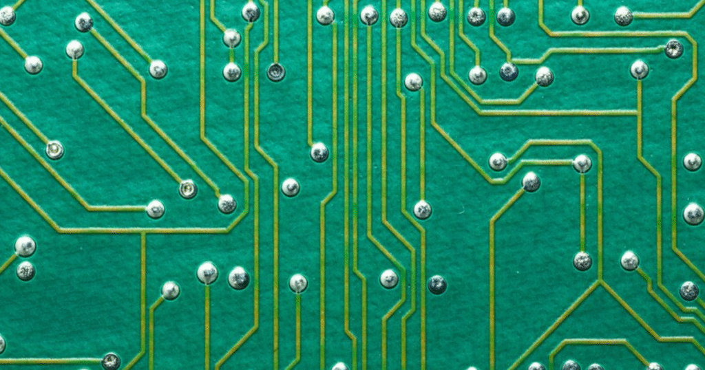
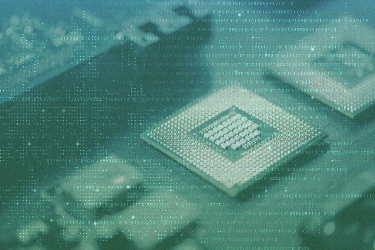
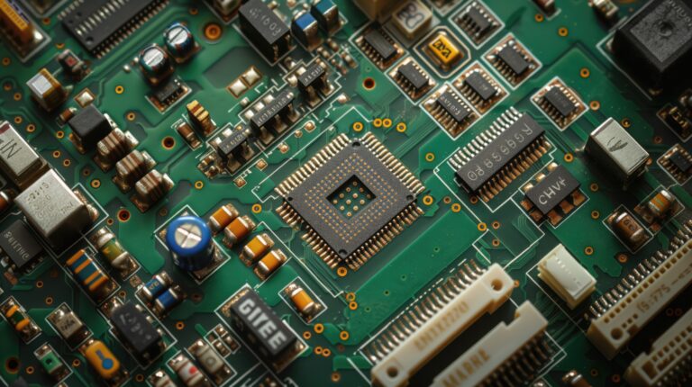
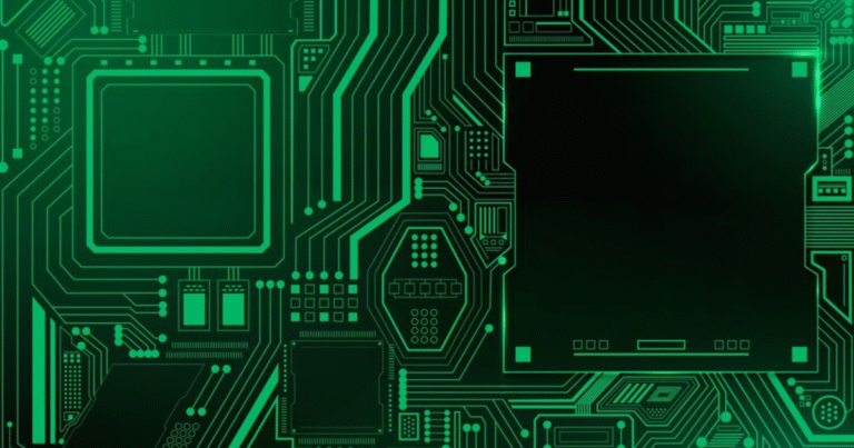
At the heart of every electronic device lies a critical component that ensures seamless functionality: the Printed Circuit Board (PCB). A PCB is a flat, sturdy board crafted from insulating materials such as fiberglass or composite epoxy, with intricate conductive pathways—typically made of copper—etched or printed onto its surface. These pathways serve as the highways for electrical signals, connecting components like resistors, capacitors, integrated circuits (ICs), and more to create a fully operational circuit.

PCBs are ubiquitous, powering everything from everyday gadgets like smartphones, laptops, and smartwatches to sophisticated systems in medical equipment, aerospace technology, and industrial machinery. By replacing cumbersome wiring with a compact and organized structure, PCBs enable manufacturers to build reliable, efficient, and space-saving circuits that drive modern innovation.

This comprehensive guide dives deep into the world of PCBs, covering their structure, types, manufacturing process, and advanced concepts. Whether you’re a hobbyist, engineer, or business owner, you’ll gain a clear understanding of why PCBs are indispensable and how they shape the electronics industry. Here’s what we’ll explore:

  • The fundamental structure of a PCB and its core components
  • Various types of PCBs and their unique applications
  • A detailed, step-by-step look at the PCB manufacturing process
  • Characteristics that define a high-quality PCB
  • Advanced PCB technologies, including solder masks, prepreg, and High-Density Interconnect (HDI) designs
  • Emerging trends and future innovations in PCB technology

How Does a PCB Work?

How Does a PCB Work

A PCB serves as both a physical platform and an electrical roadmap for electronic components. It holds components securely in place while its copper pathways—known as traces—act like wires, enabling the flow of power and signals between them. This organized connectivity ensures that devices function as intended, whether they’re processing data, amplifying signals, or powering displays.

The elegance of a PCB lies in its simplicity and efficiency. By consolidating complex circuitry onto a single board, it eliminates the need for tangled wires and reduces the risk of electrical faults. The result is a compact, durable, and highly reliable solution that can be mass-produced for consumer electronics or customized for specialized applications.

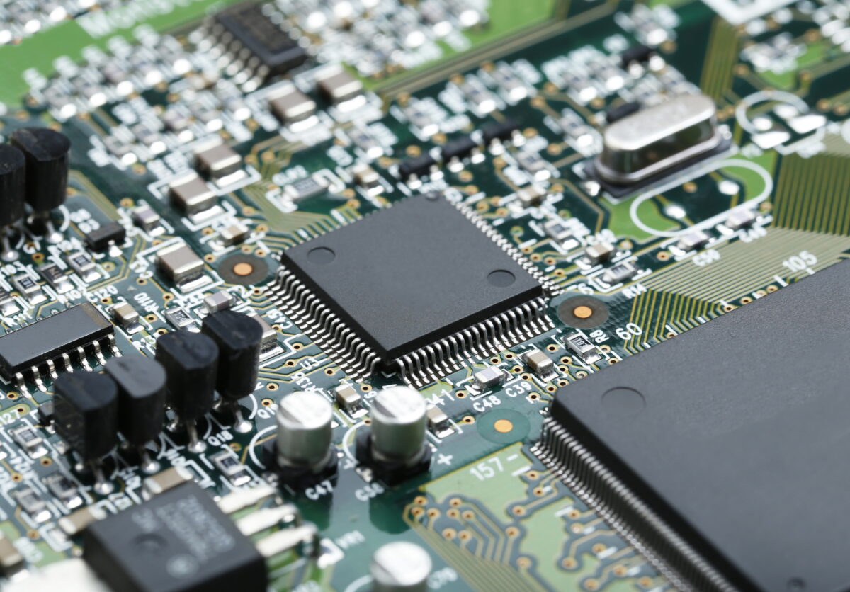
Key Elements of a PCB

To understand how a PCB functions, let’s break down its essential components:

  • Substrate (Base Material): The foundation of a PCB, typically made from FR4, a fiberglass-reinforced epoxy that offers strength, insulation, and heat resistance. For specialized applications, materials like aluminum or polyimide may be used.
  • Copper Layer: Thin sheets of copper are laminated onto one or both sides of the substrate. These are etched to form the conductive traces that carry electrical signals.
  • Solder Mask: A protective polymer layer, often green but available in colors like blue or black, coats the copper traces to prevent short circuits, oxidation, and environmental damage.
  • Silkscreen: This layer adds printed labels, symbols, or logos to the PCB, guiding assembly by indicating component placement and orientation.

Together, these elements create a robust and functional board that can support a wide range of electronic applications.

Common Materials Used for PCB Layout Construction

Material Selection

The choice of material is a foundational aspect of PCB layout, as it affects the board’s electrical properties, thermal behavior, and durability. Different materials are selected based on the application’s requirements, such as flexibility, heat dissipation, or high-frequency performance. Below are the most commonly used materials:

  • FR-4: A fiberglass-reinforced epoxy laminate, FR-4 is the industry standard for rigid PCBs. It offers a balance of strength, insulation, and affordability, making it ideal for most consumer and industrial applications.
  • Polyimide: Used in flexible PCBs, polyimide provides excellent heat resistance and bendability. It’s perfect for wearable devices, foldable electronics, and applications requiring dynamic movement.
  • Teflon (PTFE): Known for its low dielectric constant, Teflon is used in high-frequency PCBs, such as those in radio and microwave systems, where signal integrity is paramount.
  • Metal-Core PCBs: These boards feature a metal substrate, typically aluminum, to enhance thermal management. They’re used in high-power applications like LED lighting and automotive electronics.

Each material brings unique advantages, and selecting the right one ensures the PCB meets the electrical, mechanical, and environmental demands of its intended use.

Types of PCBs

PCBs are not one-size-fits-all; they come in various forms tailored to specific needs and industries. The choice of PCB type depends on factors like circuit complexity, size constraints, and environmental conditions. Below, we explore the most common types and their applications.

Single-Layer PCBs

The simplest form of PCB, a single-layer board features one conductive copper layer on a substrate. These boards are cost-effective and ideal for basic electronics, such as calculators, power supplies, or low-cost consumer devices. Their straightforward design makes them easy to manufacture and assemble, but they lack the capacity for complex circuits.

Double-Layer PCBs

Double-layer PCBs have copper layers on both sides of the substrate, connected by small holes called vias. This design allows for more intricate circuits, making them suitable for applications like automotive dashboards, LED lighting systems, and home appliances. The added flexibility of dual-sided connections supports moderately complex designs without significantly increasing costs.

Multi-Layer PCBs

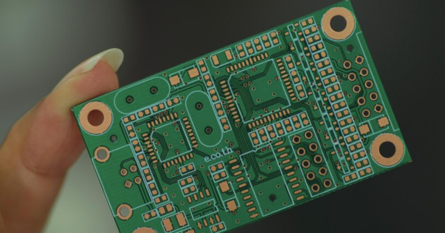
For high-performance electronics, multi-layer PCBs are the go-to choice. These boards consist of four or more copper layers separated by insulating materials, enabling dense and sophisticated circuitry. They power advanced devices like smartphones, servers, medical imaging systems, and telecommunications equipment. The layered structure enhances signal integrity and supports high-speed data transfer, but it requires precise manufacturing.

Flexible PCBs

Unlike rigid PCBs, flexible PCBs are made from bendable materials like polyimide, allowing them to conform to unique shapes or fit into tight spaces. These boards are essential for wearable technology, foldable smartphones, and aerospace systems where weight and flexibility are critical. Their ability to withstand vibration and bending makes them durable in dynamic environments.

Rigid-Flex PCBs

Rigid-flex PCBs combine the best of both worlds: rigid sections for structural support and flexible sections for adaptability. This hybrid design is used in applications like military equipment, medical implants, and advanced robotics, where reliability and compactness are paramount. By reducing the need for connectors and cables, rigid-flex PCBs enhance durability and streamline assembly.

High-Density Interconnect (HDI) PCBs

HDI PCBs represent the pinnacle of miniaturization, featuring ultra-fine traces, micro-vias, and high component density. These boards are critical for cutting-edge electronics like 5G devices, IoT sensors, and compact medical devices. Their ability to pack more functionality into smaller spaces drives innovation in industries where size and performance are non-negotiable.

The PCB Manufacturing Process (Step-by-Step)

Creating a PCB is a meticulous process that blends engineering precision with advanced technology. Each step is carefully executed to ensure the board meets strict performance and reliability standards. Here’s a detailed look at how PCBs are made.

1. Design & Schematic Capture

The journey begins with circuit design, where engineers use specialized software like Altium Designer, KiCad, or Eagle to create a schematic of the circuit. This blueprint outlines how components will connect and function. Once finalized, the schematic is converted into Gerber files—a universal format that guides the manufacturing process by specifying the board’s layout, layers, and features.

2. Material Selection & Sheet Cutting

The choice of base material is critical, as it affects the PCB’s durability, thermal performance, and electrical properties. FR4 is the most common substrate for rigid PCBs, while polyimide is used for flexible boards and aluminum for heat-dissipating applications. The selected material is cut into precise sizes using automated machinery, preparing it for further processing.

3. CNC Drilling

Precision drilling creates holes for component leads and vias, which connect different layers of the PCB. Computer Numerical Control (CNC) machines ensure accuracy, as even minor deviations can disrupt connectivity. Vias are later plated to establish electrical pathways between layers.

4. Plating Through Holes (PTH)

To enable inter-layer connections, drilled holes are electroplated with a conductive material, typically copper. This process, known as Plating Through Holes (PTH), ensures robust electrical pathways across the board, especially in multi-layer designs.

5. Photolithography & Etching

The circuit pattern is formed through photolithography, where a photosensitive dry film is applied to the copper layer. The film is exposed to ultraviolet (UV) light through a mask, hardening the areas that will become traces. Unwanted copper is then etched away using chemical solutions, leaving behind the precise conductive pathways.

6. Solder Mask Application

A protective solder mask is applied to shield the copper traces from environmental damage and prevent unintended solder connections during assembly. Available in various colors (green being the most common), the solder mask enhances the board’s longevity and reliability.

7. Silkscreen Printing

The silkscreen layer adds visual clarity by printing labels, component identifiers, and logos onto the PCB. This step aids technicians during assembly and troubleshooting, ensuring components are placed correctly.

8. Surface Finish Application

A surface finish is applied to exposed copper areas to enhance solderability and protect against oxidation. Common finishes include:

  • HASL (Hot Air Solder Leveling): A cost-effective option that coats the board with molten solder, ideal for traditional applications.
  • ENIG (Electroless Nickel Immersion Gold): A premium finish that supports fine-pitch components and ensures excellent conductivity.
  • OSP (Organic Solderability Preservative): An eco-friendly choice for consumer electronics, offering a thin protective layer.

Each finish is chosen based on the PCB’s intended use and performance requirements.

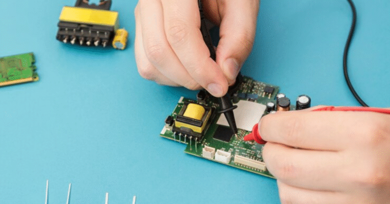
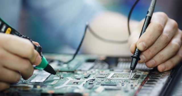
9. Electrical Testing (Flying Probe / AOI)

Quality assurance is critical. Automated Optical Inspection (AOI) scans the board for visual defects, while Flying Probe Testing checks electrical connectivity by probing specific points. These tests identify issues like open circuits or shorts before the board moves to assembly.

10. Final Cutting & Packaging

The finished PCBs are cut into individual units using CNC routing or V-scoring, a technique that creates grooves for easy separation. The boards are then cleaned, inspected, and packaged for shipment to assembly facilities or customers.

What Makes a High-Quality PCB?

What Makes a High-Quality PCB?

A high-quality PCB is defined by its reliability, performance, and durability. Manufacturers strive to achieve perfection in every aspect of the board, as even minor flaws can lead to device failure. Key characteristics of a superior PCB include:

  • Precision in Traces and Pads: Clean, accurate traces and pads ensure consistent electrical performance without shorts or broken connections.
  • Proper Layer Alignment: In multi-layer PCBs, precise alignment prevents signal interference and maintains circuit integrity.
  • Effective Solder Mask Coverage: A well-applied solder mask protects against corrosion, environmental stress, and unintended solder bridges.
  • Robust Plated Through-Holes (PTHs): Strong, conductive vias ensure reliable connections between layers, even under thermal or mechanical stress.
  • Superior Thermal Management: High-quality PCBs dissipate heat effectively, preventing damage in power-intensive applications.

By adhering to strict design and manufacturing standards, top-tier PCBs deliver consistent performance in demanding environments.

Advanced PCB Concepts

As electronics evolve, so do PCBs, incorporating advanced materials and techniques to meet modern demands. Let’s explore some key concepts driving innovation.

What is Prepreg in PCBs?

Prepreg, short for pre-impregnated fiberglass, is a critical material in multi-layer PCBs. It consists of fiberglass cloth soaked in an uncured resin, which remains pliable until heated during the lamination process. When pressed and heated, prepreg bonds the core layers of a PCB, providing insulation and structural stability. Its ability to fill gaps and ensure uniform bonding makes it essential for complex, high-layer-count boards.

What is a Solder Mask?

The solder mask is more than just a colorful coating; it’s a protective polymer layer that safeguards the PCB’s copper traces. By preventing solder bridges, oxidation, and damage from dust or moisture, the solder mask extends the board’s lifespan. While green is the traditional color, manufacturers now offer blue, red, black, and even white solder masks to suit aesthetic or functional needs.

HDI & UHDI PCBs

High-Density Interconnect (HDI) PCBs are designed for compact, high-performance electronics. They feature micro-vias (tiny holes less than 150µm in diameter), ultra-fine traces, and densely packed components, enabling smaller, lighter devices without sacrificing functionality. HDI boards are vital for applications like 5G smartphones, IoT devices, and medical wearables.

Taking it a step further, Ultra-High Density Interconnect (UHDI) PCBs push the boundaries with traces finer than 15µm and even smaller vias. UHDI technology is paving the way for next-generation electronics, where miniaturization and speed are critical.

Emerging Trends in PCB Technology

The PCB industry is constantly evolving to keep pace with technological advancements. Some exciting trends shaping the future include:

  • Embedded Components: By embedding passive components like resistors and capacitors within the PCB’s layers, manufacturers can reduce size and improve performance. This approach is gaining traction in aerospace and medical devices.
  • Sustainable Materials: As environmental concerns grow, manufacturers are exploring eco-friendly substrates and lead-free finishes to reduce the ecological footprint of PCBs.
  • 3D-Printed PCBs: Additive manufacturing is revolutionizing PCB prototyping, allowing engineers to create complex, custom boards with unprecedented speed and flexibility.
  • AI-Driven Design: Artificial intelligence is streamlining PCB design by optimizing layouts, predicting performance issues, and reducing time-to-market for new products.

These innovations highlight the dynamic nature of PCB technology, ensuring it remains at the forefront of electronic innovation.

Conclusion: Why PCBs Are Essential in Modern Electronics

Printed Circuit Boards are the unsung heroes of the electronics world, enabling everything from pocket-sized gadgets to mission-critical systems. Their ability to combine compactness, reliability, and versatility has made them indispensable across industries. As technology advances, PCBs continue to evolve, incorporating cutting-edge materials, designs, and manufacturing techniques to meet the demands of tomorrow’s devices.

At Megabyte Circuit, we’re passionate about bringing your ideas to life with high-quality prototype PCBs in Ahmedabad. Whether you’re a startup developing a groundbreaking product or an engineer refining a complex design, our precision manufacturing and expert guidance ensure your PCBs meet the highest standards.

Ready to start your PCB project? Contact us today to explore custom solutions tailored to your needs!

Categories
PCB Guide

PCB Components: A Complete Guide to Mastering Soldering and Preventing Short Circuits

PCB Components: A Complete Guide to Mastering Soldering and Preventing Short Circuits

Printed Circuit Boards (PCBs) are the unsung heroes of modern electronics, silently powering devices from smartphones to spacecraft. At their core, PCBs rely on a carefully orchestrated ensemble of components, each contributing to the board’s functionality. However, the performance of a PCB hinges not only on the selection of these components but also on their precise placement, secure connections, and protection against issues like short circuits. This comprehensive guide explores the world of PCB components, offering insights into their roles, effective soldering techniques, and strategies to prevent short circuits. Whether you’re a hobbyist tinkering with DIY projects or an engineer designing cutting-edge technology, mastering these fundamentals will elevate your PCB projects to new heights.

This guide will walk you through the essentials of PCB components, from their basic functions to advanced assembly techniques. You’ll learn how to choose the right materials, identify and place components correctly, connect them seamlessly, and troubleshoot common issues like short circuits. By the end, you’ll have a solid foundation for creating reliable, high-performance PCBs that stand the test of time.

What Are PCB Components?

PCB components are the individual elements that bring a circuit board to life. Each component serves a specific electrical purpose, such as controlling current, storing energy, or processing signals. From the humble resistor to the sophisticated integrated circuit (IC), these components work in harmony to execute the tasks defined by the circuit’s design. Without them, a PCB would be nothing more than a lifeless slab of material.

Components vary widely in complexity and function. Some, like resistors and capacitors, perform simple tasks, while others, like microprocessors, handle intricate computations. The choice of components depends on the device’s requirements, whether it’s a low-cost consumer gadget or a high-reliability medical system. Understanding the role of each component is the first step toward building a functional and efficient PCB.

Understanding PCB Materials

what is PCB Layout

The foundation of any PCB is its material, which influences how components are mounted, how the board handles heat, and how it performs under stress. The most common substrate is FR4, a fiberglass-reinforced epoxy that offers a balance of strength, insulation, and affordability. For flexible PCBs, polyimide is preferred due to its bendability, making it ideal for wearable devices or compact electronics. In high-power applications, aluminum substrates excel at dissipating heat, protecting components from thermal damage.

The choice of material impacts not only the board’s physical properties but also its electrical behavior. For instance, FR4 provides excellent insulation, preventing unwanted current flow between traces, while polyimide supports dynamic applications where flexibility is key. Additionally, the solder mask—a protective layer applied over copper traces—shields components from environmental factors like moisture and dust. Selecting the right material ensures that components are securely mounted and that the PCB operates reliably under its intended conditions.

Key PCB Components and Their Functions

PCBs host a variety of components, each with a unique role in the circuit. Below, we explore the most common components and their functions, providing a clear picture of how they contribute to a PCB’s operation.

Resistors limit the flow of electric current, protecting sensitive components from overload. They’re essential in applications like LED circuits, where excessive current could cause damage.

Capacitors store and release electrical energy, acting like tiny batteries. They stabilize power supplies, filter out noise, and smooth voltage fluctuations in circuits.

Inductors store energy in a magnetic field when current flows through them. They’re commonly used in power supplies and radio frequency circuits to filter signals.

Diodes ensure current flows in one direction, safeguarding circuits from reverse voltage. They’re critical in power supplies and signal processing.

Transistors function as switches or amplifiers, controlling current flow based on input signals. They’re the backbone of digital circuits and amplifiers.

Integrated Circuits (ICs) are miniature powerhouses, combining thousands of components into a single chip. They perform complex tasks like data processing, memory storage, and signal modulation.

Transformers transfer energy between circuits via electromagnetic induction, enabling voltage conversion in power supplies.

Switches allow manual control of a circuit by opening or closing electrical paths, commonly used in user interfaces.

Voltage Regulators maintain consistent voltage levels, protecting components from spikes or drops in power.

Silicon-Controlled Rectifiers (SCRs) act as controlled switches in high-voltage applications, such as motor controls.

Crystal Oscillators generate precise clock signals for timing, ensuring synchronization in microcontrollers and communication devices.

LEDs (Light-Emitting Diodes) produce light when current flows through them, serving as indicators or displays in electronics.

Each component is carefully selected to meet the circuit’s electrical and physical requirements, ensuring optimal performance.

How to Identify PCB Components Correctly

Identifying components on a PCB is a critical skill for assembly, repair, and troubleshooting. Most PCBs use a silkscreen layer to print reference designators—letters like “R” for resistors, “C” for capacitors, and “U” for ICs—next to each component. These designators, combined with part numbers or ratings, provide a roadmap for understanding the board’s layout.

For example, a resistor might be labeled “R1” with a value like “10k” (10,000 ohms) printed nearby. Capacitors may include capacitance values (e.g., “100µF”) or voltage ratings. ICs often carry part numbers, which can be cross-referenced with datasheets to confirm their function. During repairs, a magnifying glass or multimeter can help verify component identities, especially on densely packed boards. Accurate identification ensures that replacements or upgrades maintain the circuit’s integrity.

How to Place Components on a PCB

Effective component placement is a blend of engineering precision and practical considerations. Poor placement can lead to signal interference, overheating, or manufacturing challenges, while thoughtful placement enhances performance and reliability. Key principles include:

  • Proximity to Connectors: Place critical components, like microcontrollers or power regulators, near connectors to minimize signal loss.
  • Thermal Management: Keep heat-sensitive components away from power-hungry parts, such as transistors or voltage regulators, to prevent thermal damage.
  • Signal Integrity: Arrange components to shorten trace lengths, reducing noise and improving high-speed performance.
  • Manufacturing Efficiency: Group similar components together to streamline assembly, especially for automated pick-and-place machines.

PCB design software, such as Altium or KiCad, allows engineers to simulate placements and optimize layouts before production. By balancing electrical, thermal, and physical constraints, proper placement ensures a robust and efficient PCB.

How PCB Components Are Connected

Components on a PCB are linked through a network of copper traces, vias, pads, and landings, forming the circuit’s electrical pathways. Copper traces act as conductive highways, carrying signals and power between components. Vias—small, plated holes—enable connections between layers in multi-layer PCBs, allowing complex circuits to fit in compact spaces. Pads and landings provide surfaces for soldering component leads, ensuring secure electrical and mechanical bonds.

Two primary mounting technologies dominate PCB assembly:

  • Through-Hole Technology (THT): Components are inserted into drilled holes and soldered on the opposite side. THT is durable and ideal for high-power or mechanical components but requires more space.
  • Surface-Mount Technology (SMT): Components are soldered directly onto the board’s surface, enabling smaller, denser designs. SMT dominates modern electronics due to its compactness and automation compatibility.

Advanced PCB design software simulates connections, catching errors like open circuits or incorrect routings before manufacturing begins. This ensures reliable connectivity across the board.

Causes of Short Circuits on a PCB and How to Prevent Them

Short circuits are a common PCB failure mode, occurring when unintended connections form between traces, pads, or components. This can lead to malfunctions, overheating, or permanent damage. Common causes include:

  • Solder Bridges: Excess solder can connect adjacent pads, creating unwanted pathways.
  • Damaged Traces: Physical stress or manufacturing defects may cause traces to crack or touch.
  • Contaminants: Dust, moisture, or conductive debris on the board can bridge connections.
  • Design Errors: Incorrect layouts or insufficient spacing between traces increase short-circuit risks.

Preventing short circuits requires diligence at every stage:

  • Thorough Inspection: Visually check solder joints and use automated optical inspection (AOI) to catch defects.
  • Solder Mask Application: A well-applied solder mask insulates traces, reducing the risk of accidental connections.
  • Clean Environments: Assemble PCBs in dust-free, dry conditions to avoid contamination.
  • Design Validation: Use Electronic Design Automation (EDA) tools to verify trace spacing and layout integrity before production.

By addressing these risks, you can significantly enhance your PCB’s reliability. 

Mastering Soldering Techniques for PCB Assembly

Soldering is the art of joining components to a PCB, and mastering it is essential for creating durable, functional boards. A well-executed solder joint ensures strong electrical and mechanical connections, while poor soldering can lead to failures. Here’s how to excel at soldering:

  • Choose the Right Tools: Invest in a temperature-controlled soldering iron (25–40W for general use), fine-tipped nozzles, and high-quality solder wire (typically 60/40 tin-lead or lead-free alternatives).
  • Prepare Surfaces: Clean component leads and PCB pads with isopropyl alcohol to remove oxidation or debris, ensuring a strong bond.
  • Control Heat: Set the iron to 300–350°C for most electronics. Too much heat can damage components, while too little results in weak joints.
  • Apply Proper Technique: Heat the pad and component lead simultaneously for 1–2 seconds, then introduce solder. Let it flow naturally to form a smooth, cone-shaped joint. Avoid excessive solder to prevent bridges.
  • Inspect Joints: Ideal joints are shiny, uniform, and tapered. Dull, cracked, or lumpy joints indicate issues and should be reworked.

For advanced projects, explore techniques like drag soldering for multi-pin ICs, reflow soldering using solder paste and ovens, or hot air rework for surface-mount components. Practice and attention to detail will refine your skills, ensuring professional-grade results.

Factors to Consider When Choosing PCB Components

what is PCB Layout

Selecting the right components is a critical step in PCB design, balancing performance, cost, and practicality. Key considerations include:

  • Electrical Specifications: Ensure components meet the circuit’s voltage, current, power, and frequency requirements. For example, a capacitor’s voltage rating must exceed the circuit’s maximum voltage.
  • Physical Size and Footprint: Components must fit the PCB’s layout and available space, especially in compact designs.
  • Reliability and Quality: Choose components from reputable manufacturers that meet industry standards, such as IPC or JEDEC.
  • Material Compatibility: Verify that components are suitable for the PCB’s material and soldering process (e.g., lead-free soldering requires compatible finishes).
  • Availability: Check stock levels and lead times to avoid delays, especially for specialized components.
  • Cost: Balance performance with budget constraints, opting for cost-effective alternatives when possible.
  • Compliance: Ensure components meet regulatory requirements, such as RoHS for environmental safety or UL for fire resistance.
  • Interoperability: Confirm that components work seamlessly with other parts of the system, avoiding compatibility issues.
  • Future-Proofing: Select components with long-term availability or multiple sourcing options to prevent obsolescence.

By carefully evaluating these factors, you can build a PCB that meets both immediate needs and long-term goals.

Conclusion

Mastering PCB components, soldering techniques, and short-circuit prevention is a journey that combines technical knowledge with hands-on skill. From selecting the right resistors and capacitors to perfecting solder joints and validating designs, every step demands precision and care. By understanding the roles of components, optimizing their placement, and safeguarding against issues like short circuits, you can create PCBs that are reliable, efficient, and built to last.

Whether you’re assembling a prototype in a garage or designing a commercial product, these principles will guide you toward success. At Megabyte Circuit, we’re committed to supporting your PCB projects with high-quality manufacturing and expert advice. Ready to take your electronics to the next level? Contact us today to bring your vision to life!

Categories
PCB Guide

What is PCB Layout? A Comprehensive Guide

What is PCB Layout? A Comprehensive Guide

Printed Circuit Boards (PCBs) are the cornerstone of modern electronics, enabling everything from smartphones to satellite systems. At the heart of every PCB lies its layout a meticulously planned arrangement of components and electrical connections on a non-conductive board. The PCB layout is far more than a technical diagram; it’s a critical blueprint that determines a device’s performance, reliability, and manufacturability. A well-executed layout ensures seamless operation, while a flawed one can lead to costly failures. This guide explores the intricacies of PCB layout, from its fundamental principles to advanced applications, offering insights for hobbyists, engineers, and industry professionals alike.

In this comprehensive guide, we’ll dive into the materials, processes, and considerations that shape PCB layouts. You’ll learn about the design process, manufacturing steps, real-world applications, and emerging trends that are redefining the field. Whether you’re designing a simple prototype or a complex aerospace system, understanding PCB layout is essential to creating electronics that perform flawlessly.

Overview of PCB Layout

Understanding PCB Materials

What is PCB Layout?

PCB layout is the art and science of arranging electronic components and their interconnections on a board made of insulating material, such as fiberglass or polyimide. It transforms an electrical schematic a conceptual diagram of how components connect into a physical structure that can be manufactured and assembled. The layout process requires balancing electrical performance, mechanical constraints, and thermal management to create a board that is functional, reliable, and cost-effective.

A successful PCB layout minimizes signal interference, optimizes heat dissipation, and ensures the board can be produced efficiently. It serves as the bridge between design and reality, guiding manufacturers through every step of fabrication and assembly. From consumer gadgets to mission-critical medical devices, the precision of the PCB layout directly impacts the success of the final product.

Common Materials Used for PCB Layout Construction

Material Selection

The choice of material is a foundational aspect of PCB layout, as it affects the board’s electrical properties, thermal behavior, and durability. Different materials are selected based on the application’s requirements, such as flexibility, heat dissipation, or high-frequency performance. Below are the most commonly used materials:

  • FR-4: A fiberglass-reinforced epoxy laminate, FR-4 is the industry standard for rigid PCBs. It offers a balance of strength, insulation, and affordability, making it ideal for most consumer and industrial applications.
  • Polyimide: Used in flexible PCBs, polyimide provides excellent heat resistance and bendability. It’s perfect for wearable devices, foldable electronics, and applications requiring dynamic movement.
  • Teflon (PTFE): Known for its low dielectric constant, Teflon is used in high-frequency PCBs, such as those in radio and microwave systems, where signal integrity is paramount.
  • Metal-Core PCBs: These boards feature a metal substrate, typically aluminum, to enhance thermal management. They’re used in high-power applications like LED lighting and automotive electronics.

Each material brings unique advantages, and selecting the right one ensures the PCB meets the electrical, mechanical, and environmental demands of its intended use.

Key Highlights of PCB Layout

A Multidisciplinary Blueprint

PCB layout is a convergence of electrical engineering, mechanical design, and manufacturing expertise. It must accommodate the circuit’s electrical needs such as signal integrity and power distribution while fitting within the mechanical constraints of the device’s size and shape. Additionally, the layout must align with manufacturing processes, ensuring the board can be produced efficiently and tested for quality.

The layout process generates critical documentation, including Gerber files (which define the board’s layers), drill files (specifying hole locations), and the Bill of Materials (BOM, listing components). These files guide manufacturers, minimizing errors and ensuring the final PCB matches the designer’s vision. A well-crafted layout enhances reliability, reduces production costs, and supports long-term performance.

PCB Layout Design Considerations

Balancing Multiple Factors

Designing a PCB layout requires careful consideration of several factors, each influencing the board’s performance and manufacturability. Ignoring these can lead to signal issues, overheating, or production challenges. Key considerations include:

  • Electrical Performance: Signal integrity, impedance matching, and noise reduction are critical for high-speed or sensitive circuits. Proper trace routing and component placement minimize interference.
  • Mechanical Constraints: The board’s size, shape, and mounting points must align with the device’s enclosure. Structural stability is also essential to withstand vibrations or shocks.
  • Thermal Management: Heat-generating components, like processors or power regulators, must be positioned to avoid hotspots. Thermal vias and heatsinks can enhance heat dissipation.
  • Manufacturability: The layout should support automated assembly and testing, with adequate spacing for pick-and-place machines and test probes.
  • Cost: Efficient layouts reduce costs by minimizing board layers, optimizing material use, and simplifying assembly.

Balancing these factors requires expertise and often involves trade-offs. For example, a smaller board may save space but complicate thermal management. Design software helps engineers simulate and refine layouts to achieve the best outcome.

Designing a PCB Layout

Step-by-Step Process

Creating a PCB layout is a structured process that transforms a schematic into a manufacturable board. Each step demands precision to ensure the final product meets its specifications.

1. Schematic Design

The process begins with a schematic a logical diagram showing how components connect electrically. Created using software like Altium, KiCad, or Eagle, the schematic serves as the roadmap for the layout. It defines component relationships and helps identify potential errors, such as incorrect connections, before moving to the physical design.

2. Component Placement

Placing components is a critical step that affects signal integrity, thermal performance, and usability. High-frequency components, like RF modules, are positioned to minimize trace lengths and avoid interference. Power components require space for heatsinks or thermal vias. User-facing elements, such as connectors or buttons, must be accessible within the device’s enclosure. Design software allows engineers to experiment with placements, ensuring optimal performance.

3. Trace Routing

Routing involves drawing copper traces to connect components, forming the circuit’s electrical pathways. Trace width and spacing are tailored to handle current loads and prevent short circuits. For high-speed signals, impedance matching and equal-length traces are crucial to avoid delays or noise. In multi-layer boards, vias connect traces across layers, requiring careful layer management to optimize space and performance.

4. Gerber Generation

Once the layout is finalized, Gerber files are generated. These files describe the board’s layers, including copper traces, solder masks, and silkscreen markings. Drill files specify hole locations, and the BOM lists all components. Accuracy is paramount, as errors in Gerber files can lead to defective boards. Most design software includes validation tools to catch issues before submission to manufacturers.

what is PCB Layout

PCB Manufacturing

From Layout to Reality

The PCB layout guides the manufacturing process, which transforms raw materials into a functional board. Each step requires precision to ensure the board matches the design.

1. Surface Preparation

The base material, such as FR-4 or polyimide, is cleaned to remove contaminants. A pristine surface ensures strong adhesion for copper layers and coatings, preventing defects during fabrication.

2. Teflon Coating

For high-frequency PCBs, a Teflon-based coating may be applied to reduce signal loss and enhance transmission. This step is common in RF and microwave applications, where low dielectric constants are critical.

3. Copper Cladding

Thin copper sheets are laminated onto the board, forming the conductive pathways. The copper is later etched to create the traces defined in the layout.

4. Drilling

CNC machines drill precise holes for vias (connecting layers) and component leads. Even minor misalignments can disrupt connectivity, making accuracy essential.

5. Lamination

In multi-layer PCBs, individual layers are stacked, aligned, and pressed together under heat and pressure. Prepreg (resin-soaked fiberglass) bonds the layers, creating a unified board.

6. Outer Layer Imaging and Etching

The outer layers are coated with a photosensitive film, exposed to UV light through a mask, and developed to reveal the circuit pattern. Unwanted copper is etched away, leaving the final traces.

7. Inspection and Testing

Finished PCBs undergo Automated Optical Inspection (AOI) to detect visual defects and electrical testing (e.g., Flying Probe) to verify connectivity. These steps ensure the board meets design specifications before assembly.

PCB Layout Applications

Real-World Uses

PCB layouts are tailored to the needs of specific industries, each with unique requirements for performance and reliability.

1. Radio and Microwave Systems

RF and microwave PCBs require specialized layouts to maintain signal fidelity at high frequencies. Materials like Teflon and precise trace routing minimize signal loss and electromagnetic interference (EMI), making them ideal for communication devices and radar systems.

2. Aerospace and Automotive Devices

These sectors demand PCBs that withstand extreme temperatures, vibrations, and mechanical stress. Layouts prioritize durability, with robust materials and redundant connections to ensure reliability in harsh environments.

3. Medical Devices and Industrial Control Systems

Precision and safety are paramount in medical and industrial PCBs. Layouts for devices like pacemakers or factory automation systems focus on signal accuracy, longevity, and compliance with strict regulations.

PCB Layout Maintenance and Repair

Ensuring Longevity

Even the best PCBs require maintenance over time. Repairs involve diagnosing issues like broken traces or faulty components, often using multimeters or oscilloscopes. Damaged components can be replaced, and traces may be reworked with solder or conductive ink. Regular maintenance, such as cleaning to remove dust or corrosion, extends the board’s lifespan and reduces downtime in critical applications.

Advantages of Using PCB Layout

Why Layout Matters

A well-designed PCB layout offers numerous benefits that enhance device performance and production efficiency.

1. Durability and Reliability

Thoughtful layouts ensure PCBs withstand mechanical stress, temperature fluctuations, and environmental factors, reducing the risk of failure.

2. Thermal Management

Strategic component placement and thermal vias keep temperatures in check, protecting components from overheating and extending device life.

3. Signal Integrity

Optimized trace routing minimizes crosstalk, EMI, and signal loss, ensuring high-speed circuits perform reliably.

4. Early Detection and Fixing

Layout design tools catch errors before manufacturing, saving time and costs compared to post-production fixes.

5. Enabling Innovation

Advanced layouts support cutting-edge technologies like IoT, 5G, and wearable devices, enabling compact and powerful designs.

PCB Layout Challenges

Overcoming Obstacles

Designing PCB layouts is not without challenges, especially as electronics become smaller and more complex.

1. Demand for Miniaturization

Shrinking devices require fitting intricate circuits into tiny spaces, complicating trace routing and component placement.

2. High-Speed Signal Transmission

High-frequency designs demand precise impedance control and noise reduction, requiring advanced materials and routing techniques.

3. Specialized Equipment

Modern PCBs rely on sophisticated tools for imaging, drilling, and testing, which can be costly and require skilled operators.

4. High Cost

Complex layouts, such as multi-layer or flexible designs, increase production costs, particularly for low-volume runs.

PCB Layout Future Directions

The Road Ahead

The future of PCB layout is bright, with innovations poised to transform the field. Artificial intelligence (AI) is streamlining design by optimizing layouts and predicting performance issues. Flexible and biodegradable substrates are enabling eco-friendly and wearable electronics. 3D-printed PCBs offer rapid prototyping and customization, while high-speed designs for 5G and beyond push the limits of signal integrity. As these trends evolve, PCB layouts will continue to drive technological progress.

Conclusion

PCB layout is the backbone of electronic design, blending electrical functionality, mechanical precision, and manufacturing efficiency into a single blueprint. By mastering material selection, design considerations, and manufacturing processes, engineers create PCBs that power the devices shaping our world. As technology advances, the role of PCB layout will only grow, enabling innovations that redefine what’s possible.

At Megabyte Circuit, we specialize in crafting high-quality PCB layouts tailored to your needs. Whether you’re a startup or an established industry player, our expertise ensures your designs come to life with precision and reliability. Contact us today to start your next PCB project!

Categories
PCB Guide

The Critical Importance of PCB Assembly Services in Modern Electronics

The Critical Importance of PCB Assembly Services in Modern Electronics

Printed Circuit Board (PCB) assembly is the linchpin of modern electronics, transforming bare circuit boards into functional systems that power our world. By precisely mounting and soldering components, PCB assembly ensures that devices from smartphones to life-saving medical equipment perform reliably and efficiently. In an era where technology drives innovation, high-quality assembly services are non-negotiable, providing the foundation for durability, performance, and compliance with stringent industry standards.

This comprehensive guide delves into the pivotal role of PCB assembly in electronics manufacturing. We’ll explore its protective benefits, key techniques, challenges, and the value of expertise and speed in delivering superior results. Whether you’re a startup prototyping a new gadget or an enterprise scaling production, understanding PCB assembly is essential to success. Here’s what we’ll cover:

  • How PCB assembly safeguards circuits from environmental and electrical risks
  • Essential assembly techniques, including SMT, through-hole, and conformal coating
  • Common challenges in PCB assembly and strategies to overcome them
  • The importance of experienced assembly partners
  • The advantages of quick-turnaround services
  • Tips for choosing the right PCB assembly provider

The Significance of PCB Assembly in Circuit Board Protection

Beyond Connectivity: A Shield for Electronics

PCB assembly is more than just soldering components; it’s a critical process that enhances a circuit’s durability, signal integrity, and resilience. A well-assembled PCB protects against physical, environmental, and electrical stressors, ensuring long-term performance in demanding applications.

Protection Against Physical & Environmental Damage

Electronics face constant threats from moisture, dust, and mechanical stress. PCB assembly incorporates protective measures to counter these risks:

  • Moisture and Dust: Conformal coatings, applied post-assembly, create a barrier against humidity and particulate matter, preventing corrosion that could degrade components.
  • Thermal Stress: Precise soldering techniques minimize stress from thermal expansion, reducing the risk of cracked joints or component failure.
  • Mechanical Shock: Secure component placement and robust soldering ensure parts remain intact during vibrations, making PCBs reliable in automotive or industrial settings.

Ensuring Electrical Reliability

A properly assembled PCB maintains consistent electrical performance, avoiding common pitfalls that compromise functionality:

  • Short Circuit Prevention: Accurate solder paste application prevents solder bridges, which can cause unintended connections between traces.
  • Signal Integrity: Careful component placement and trace routing reduce electromagnetic interference (EMI), ensuring clear signal transmission.
  • Power Distribution: Stable connections deliver consistent voltage, protecting sensitive components from fluctuations.

Compliance with Industry Standards

High-quality PCB assembly adheres to rigorous standards, ensuring safety and reliability:

  • IPC-A-610: This standard defines acceptable electronic assemblies, minimizing defects and ensuring consistent quality.
  • RoHS & REACH: Compliance eliminates hazardous materials, aligning with environmental and safety regulations.

By prioritizing protection, PCB assembly lays the groundwork for electronics that perform reliably in diverse conditions.

The Significance of PCB Assembly in Circuit Board Protection

PCB Assembly Techniques for Optimal Protection

Tailored Methods for Performance and Durability

PCB assembly employs a range of techniques, each suited to specific applications and performance needs. These methods balance miniaturization, strength, and environmental resilience.

Surface Mount Technology (SMT) – The Modern Standard

SMT is the dominant assembly method in modern electronics, enabling compact, high-performance devices.

  • Process: Automated pick-and-place machines position tiny components, like resistors and ICs, directly onto the PCB’s surface. Solder paste is applied, and the board is heated in a reflow oven to form permanent connections.
  • Advantages:
    • Supports high component density, enabling smaller, lighter devices.
    • Accelerates production with automated processes, ideal for mass manufacturing.
    • Enhances performance in high-frequency applications due to shorter signal paths.

Through-Hole Technology (THT) – For Robust Connections

THT remains relevant for applications requiring mechanical strength.

  • Process: Component leads are inserted into pre-drilled holes and soldered on the opposite side, creating strong bonds.
  • Advantages:
    • Provides durable connections, ideal for high-stress environments like aerospace or military systems.
    • Simplifies manual repairs, as components can be desoldered and replaced.

Through-Hole Technology (THT) – For Robust ConnectionsMixed Assembly (SMT + THT) – Balancing Performance & Durability

Many PCBs combine SMT for compact, high-density components and THT for high-power or mechanically stressed parts. This hybrid approach optimizes both performance and reliability, catering to complex designs like automotive control units.

Conformal Coating – Extra Layer of Defense

Post-assembly, conformal coating adds a protective polymer layer to shield the PCB from environmental hazards:

  • Moisture, Dust, and Chemicals: Coatings like acrylic or silicone prevent corrosion and contamination.
  • Fungus Growth: Critical for medical or marine applications, coatings inhibit microbial growth that could degrade performance.

These techniques, when applied skillfully, ensure PCBs withstand the rigors of their operating environments.

Key Challenges in PCB Assembly & How to Overcome Them

Navigating Common Hurdles

Despite advancements in technology, PCB assembly presents challenges that can compromise quality if not addressed. Understanding these issues and implementing solutions is crucial for reliable outcomes.

Common Issues in Assembly

  • Component Misalignment: Misplaced components can cause open or short circuits, disrupting functionality.
  • Solder Defects: Issues like cold joints (weak connections), tombstoning (components lifting during reflow), or bridging (excess solder connecting pads) lead to unreliable boards.
  • Thermal Stress Cracks: Improper heating during reflow can crack solder joints or components.
  • ESD Damage: Electrostatic discharge can destroy sensitive ICs, especially during handling.

Strategies for Reliable Assembly

To mitigate these challenges, manufacturers employ advanced tools and practices:

  • Automated Optical Inspection (AOI): High-resolution cameras detect soldering defects and misaligned components early in the process.
  • X-Ray Inspection: Used for hidden solder joints, such as those under Ball Grid Array (BGA) components, ensuring flawless connections.
  • Proper Reflow Profiling: Precise temperature control during reflow prevents thermal shock, ensuring uniform soldering.
  • ESD-Safe Workstations: Grounded tools and static-dissipative surfaces protect components from electrostatic damage.

By proactively addressing these issues, assemblers deliver PCBs that meet stringent quality standards.

Why Experience Matters in PCB Assembly

The Value of Expertise

Not all PCB assembly services are created equal. Experienced providers bring a wealth of knowledge that translates into superior results, fewer defects, and optimized processes.

Precision & Fewer Defects

Seasoned assemblers excel in critical areas:

  • Solder Paste Stencil Design: Accurate stencils ensure precise solder application, reducing bridging or insufficient joints.
  • Component Placement Accuracy: Expertise in pick-and-place programming minimizes misalignment, even for tiny components.

Handling Complex Designs

Modern PCBs, such as High-Density Interconnect (HDI), flex-rigid, or high-frequency boards, demand specialized skills. Experienced providers understand the nuances of micro-vias, fine-pitch components, and impedance control, ensuring flawless execution.

Faster Troubleshooting

Veteran assemblers quickly identify and resolve issues, such as:

  • Poor Solder Wetting: Caused by contaminated surfaces or incorrect solder paste, resolved through cleaning and process adjustments.
  • Delamination: Resulting from improper lamination, mitigated by optimizing heat and pressure settings.

Cost Efficiency Through Process Optimization

Experience reduces material waste and rework, lowering costs while maintaining quality. Skilled providers also streamline workflows, delivering faster turnarounds without cutting corners.

Quick Turnaround PCB Assembly: Why Speed Matters

Speed as a Competitive Advantage

In today’s fast-paced markets, rapid PCB assembly is a game-changer, enabling businesses to innovate and respond to demand swiftly.

Benefits of Fast Assembly Services

  • Faster Time-to-Market: Quick assembly accelerates product launches, helping companies outpace competitors.
  • Iterative Prototyping: Rapid prototyping allows engineers to test and refine designs in days, not weeks.
  • Emergency Replacements: Fast production minimizes downtime in critical systems, such as industrial machinery or medical equipment.

How to Ensure Speed Without Compromising Quality

To deliver rapid results without sacrificing reliability, providers rely on:

  • Pre-Kitted Components: Maintaining an inventory of common parts reduces procurement delays.
  • Streamlined Supply Chain: Strong relationships with component suppliers ensure timely delivery.
  • Dedicated Rapid-Prototyping Lines: Separate workflows for prototypes prevent bottlenecks in bulk production.

By combining speed with precision, quick-turn services empower businesses to stay agile and competitive.

Choosing the Right PCB Assembly Partner

Right PCB Assembly Partner

Key Factors for Success

Selecting the right PCB assembly partner is critical to achieving high-quality results and meeting project deadlines. Consider these factors when evaluating providers:

Technical Capabilities

  • Equipment: Advanced SMT lines, selective soldering machines, and AOI/X-ray systems indicate a provider’s ability to handle complex assemblies.
  • Materials: Access to high-quality substrates (e.g., FR-4, polyimide) and components ensures reliable boards.

Certifications & Standards Compliance

Certifications like ISO 9001 (quality management), IPC Class 3 (high-reliability electronics), and UL (safety) demonstrate a commitment to excellence. Compliance with RoHS and REACH ensures environmentally responsible manufacturing.

Scalability

A versatile partner can handle both low-volume prototypes and high-volume production, adapting to your project’s growth.

Customer Support & Transparency

Look for providers offering:

  • Design for Manufacturing (DFM) Feedback: Suggestions to optimize designs for cost and manufacturability.
  • Real-Time Tracking: Updates on production status for peace of mind.

A responsive partner collaborates closely, ensuring your project stays on track.

Conclusion: PCB Assembly

PCB assembly is the invisible force behind the electronics that shape our lives. From shielding circuits against environmental hazards to enabling cutting-edge miniaturization, it plays a pivotal role in delivering reliable, high-performance devices. By partnering with an experienced, quality-focused assembly provider, businesses can ensure compliance, accelerate innovation, and achieve faster market entry.

At Megabyte Circuit, we’re passionate about delivering precision PCB assembly services in Ahmedabad. Our offerings include:

  • Advanced SMT and through-hole assembly for diverse applications
  • Conformal coating for enhanced environmental protection
  • Quick-turn prototyping and scalable mass production

Ready to elevate your electronics project? Contact us today for expert PCB assembly solutions tailored to your needs!

Categories
PCB Guide

Double Layer PCB: A Complete Guide to Design, Manufacturing, and Applications

Double Layer PCB: A Complete Guide to Design, Manufacturing, and Applications

In the ever-evolving world of electronics, Double Layer PCBs (Printed Circuit Boards) have emerged as a fundamental component in the design and manufacturing of modern electronic devices. These boards, also known as double-sided printed circuit boards, feature conductive copper layers on both sides, connected through vias (plated holes), allowing for more complex and compact circuit designs. 

Whether you’re an engineer designing advanced systems, a hobbyist working on a personal project, or a business developing electronic products, understanding the intricacies of double layer circuit boards is crucial. This comprehensive guide will delve into every aspect of Double Layer PCBs, from their design and manufacturing processes to their applications and advantages, providing you with the knowledge needed to make informed decisions for your projects.

Introduction to Double Layer PCBs

Double Sided PCB

A Double Layer PCB is a type of printed circuit board that consists of two conductive copper layers, one on each side of the board. These layers are interconnected through vias, which are small holes drilled into the board and plated with conductive material, allowing electrical signals to pass between the two sides. 

This dual-layer structure enables more complex circuit designs compared to single-layer boards, making double-sided PCBs a popular choice for a wide range of electronic applications.

The versatility of Double Layer PCBs lies in their ability to accommodate a higher density of components and provide better electrical performance. This makes them ideal for use in industries ranging from consumer electronics to automotive and aerospace. 

For instance, double layer circuit boards are commonly found in smartphones, laptops, automotive control systems, and medical devices. Their compact design and improved performance have made them a cornerstone of modern electronics, bridging the gap between simple single-layer boards and complex multi-layer boards.

Advantages and Disadvantages of Double Layer PCBs

When considering the use of Double Layer PCBs for your project, it’s important to weigh their advantages and disadvantages to determine if they are the right fit for your needs.

Advantages of Double Layer PCBs

One of the primary advantages of double-sided PCBs is their higher circuit density. With conductive layers on both sides of the board, these PCBs can accommodate more components and support more complex circuit designs.

This makes them ideal for applications where space is at a premium, such as in smartphones and wearable devices. Additionally, the dual-layer structure allows for a more compact design, enabling the creation of smaller and more lightweight electronic devices.

Another significant advantage of Double Layer PCBs is their improved electrical performance. The presence of two conductive layers allows for better signal integrity and reduced electromagnetic interference (EMI), which is crucial for high-frequency applications.

This makes double layer circuit boards suitable for use in advanced electronic systems, such as communication devices and industrial control systems.

Cost-effectiveness is another key benefit of Double Layer PCBs. While they are more expensive than single-layer boards, they are significantly more affordable than multi-layer boards.

This makes them an excellent choice for mid-complexity projects that require more functionality than a single-layer board can provide but do not justify the cost of a multi-layer board.

Furthermore, double-sided PCBs offer greater design flexibility, allowing engineers to create more innovative and efficient circuit layouts.

Disadvantages of Double Layer PCBs

Despite their many advantages, Double Layer PCBs also have some drawbacks that need to be considered.

One of the main challenges is the complexity of the design process. Designing a double layer PCB requires careful planning to ensure proper via placement and avoid signal interference. This can be particularly challenging for engineers who are new to PCB design or working on highly complex circuits.

Another disadvantage is the higher cost compared to single-layer boards. While double-sided PCBs are more cost-effective than multi-layer boards, they are still more expensive to produce than single-layer alternatives.

This can be a limiting factor for projects with tight budgets. Additionally, the manufacturing process for double layer circuit boards is more complex, requiring precise drilling and plating for vias.

This can lead to longer production times and higher costs, especially for small-scale production runs.

Key Design Considerations for Double Layer PCBs

Designing a Double Layer PCB requires a thorough understanding of electrical engineering principles and careful attention to detail. Here are some key considerations to keep in mind during the design process:

Layer Stackup

The arrangement of the top and bottom layers is crucial for ensuring optimal performance. Proper layer stackup helps minimize interference and improve signal integrity. For example, placing a ground plane on one side of the board can help reduce noise and provide a stable reference for signal routing. It’s also important to consider the thickness of the copper layers and the dielectric material between them, as these factors can impact the board’s electrical properties.

Component Placement

The placement of components on a double Sided PCB plays a significant role in the board’s performance. High-frequency components should be placed on one side of the board to minimize signal loss and interference. Additionally, adequate spacing between components is essential to prevent overheating and ensure reliable operation. Careful consideration should also be given to the placement of vias, as they can affect the routing of traces and the overall layout of the board.

Routing and Trace Width

The routing of traces on a double layer PCB is another critical aspect of the design process. Appropriate trace widths must be used to handle the current load and prevent overheating. Sharp angles in traces should be avoided, as they can cause signal reflection and degrade performance. Instead, use smooth curves or 45-degree angles to ensure optimal signal flow.

Via Placement

Vias are essential for connecting the two layers of a double layer PCB, but their placement must be carefully planned to avoid disrupting the circuit. Through-hole vias are commonly used for reliable connections, but blind and buried vias can also be employed in more complex designs. It’s important to ensure that vias are placed in areas that do not interfere with the routing of traces or the placement of components.

Thermal Management

Effective thermal management is crucial for ensuring the reliability and longevity of a double layer PCB. Heat sinks and thermal vias can be used to dissipate heat and prevent overheating. It’s also important to avoid placing heat-sensitive components near high-power devices, as this can lead to thermal stress and potential failure.

Manufacturing Process of Double Layer PCBs: Step-by-Step

The manufacturing process of double-sided printed circuit boards involves several steps to ensure precision and reliability. Here’s a detailed overview of the process:

1. Design and Layout

The first step in manufacturing a double layer PCB is creating a schematic diagram of the circuit. This diagram is then converted into a PCB layout using specialized design software. The layout must be carefully verified for errors and optimized for manufacturing to ensure that the final product meets the required specifications.

2. Material Selection

The choice of materials is critical for the performance and durability of the PCB. The base material, typically FR-4, is selected for its excellent electrical insulation properties and mechanical strength. Copper foil is used for the conductive layers, with the thickness of the foil chosen based on the current requirements of the circuit.

3. Printing the Circuit

The circuit design is printed onto the board using a photoresist process. A layer of photoresist material is applied to the copper foil, and the circuit pattern is transferred onto the board using UV light. The exposed areas of the photoresist are then developed, leaving behind the desired circuit pattern.

4. Etching

The next step is the etching process, where excess copper is removed from the board using a chemical solution. The photoresist protects the desired circuit traces, while the unwanted copper is dissolved, leaving behind the conductive pathways.

5. Drilling and Plating

Holes are drilled into the board for vias and component leads. These holes are then plated with copper to create electrical connections between the two layers. The plating process ensures that the vias are conductive and provide reliable connections.

6. Solder Mask Application

A solder mask is applied to the board to protect the copper traces and prevent short circuits. The solder mask is typically green, but other colors can be used for aesthetic or functional purposes. Openings in the solder mask are created for soldering components to the board.

7. Silkscreen Printing

Labels, component identifiers, and other markings are added to the board using silkscreen printing. This step helps with the assembly and troubleshooting of the PCB by providing clear identification of components and connections.

8. Testing and Quality Control

The final step in the manufacturing process is testing and quality control. Electrical tests are performed to ensure that the board functions as intended and meets the required specifications. The board is also inspected for defects, such as shorts, opens, or misaligned components, to ensure that it is ready for use.

Applications of Double Layer PCBs in Modern Electronics

Double sided PCB in Ahemedabad

Double Layer PCBs are used in a wide range of industries and applications, thanks to their versatility and performance. Here are some of the most common applications:

Consumer Electronics

In the consumer electronics industry, double-sided PCBs are used in devices such as smartphones, tablets, and laptops. Their compact design and high circuit density make them ideal for these applications, where space is at a premium and performance is critical.

Automotive Industry

The automotive industry relies on double layer circuit boards for various applications, including engine control units (ECUs), infotainment systems, and LED lighting. The durability and reliability of these PCBs make them well-suited for the harsh environments found in vehicles.

Industrial Equipment

In industrial settings, double layer PCBs are used in power supplies, control systems, and monitoring devices. Their ability to handle complex circuits and provide reliable performance makes them essential for industrial automation and control.

Medical Devices

The medical industry uses double-sided PCBs in diagnostic equipment, imaging systems, and portable medical devices like glucose meters. The precision and reliability of these PCBs are crucial for ensuring the accuracy and safety of medical devices.

Aerospace and Defense

In the aerospace and defense industries, double layer PCBs are used in avionics systems, communication devices, and navigation systems. Their ability to withstand extreme conditions and provide reliable performance makes them ideal for these critical applications.

Comparison with Single and Multi-Layer PCBs

When choosing the right type of PCB for your project, it’s important to understand the differences between single-layer, double-layer, and multi-layer boards.

Single-Layer PCBs

Single-layer PCBs are the simplest type of printed circuit board, featuring a single conductive layer on one side of the board. They are easy to design and manufacture, making them a cost-effective option for simple circuits. However, their limited circuit density and larger size make them unsuitable for more complex applications.

Double Layer PCBs

Double Layer PCBs offer a balance between simplicity and complexity, with two conductive layers that allow for more compact and efficient designs. They are more expensive than single-layer boards but provide better performance and higher circuit density. This makes them ideal for mid-complexity projects that require more functionality than a single-layer board can provide.

Multi-Layer PCBs

Multi-layer PCBs consist of three or more conductive layers, offering the highest circuit density and performance. They are used in advanced electronic systems where space and performance are critical. However, their complex design and manufacturing process make them significantly more expensive than single or double-layer boards.

Tips for Choosing the Right Double Layer PCB Manufacturer

Selecting the right manufacturer for your double layer PCB is crucial for ensuring the quality and reliability of your product. Here are some tips to help you make the right choice:

  1. Experience and Expertise: Choose a manufacturer with a proven track record in producing high-quality double-sided PCBs. Look for companies with experience in your industry and a portfolio of successful projects.
  2. Certifications: Ensure that the manufacturer complies with industry standards, such as ISO and IPC certifications. This ensures that their processes and products meet the highest quality standards.
  3. Customization Options: Look for a manufacturer that offers flexible design and material options to meet your specific requirements. This includes the ability to customize the thickness, material, and finish of the PCB.
  4. Turnaround Time: Consider the manufacturer’s production capacity and lead times to ensure that they can deliver within your project timeline. Fast turnaround times are especially important for time-sensitive projects.
  5. Customer Support: Reliable communication and technical support are essential for a smooth manufacturing process. Choose a manufacturer that offers responsive customer service and is willing to work closely with you to address any issues.

If you’re based in Ahmedabad, Gujarat, or anywhere in India, consider partnering with a local manufacturer who specializes in Double Layer PCBs. This can help reduce shipping costs and lead times while supporting local businesses.

Conclusion

Double Layer PCBs are a versatile and cost-effective solution for a wide range of electronic applications. By understanding their design, manufacturing process, and advantages, you can make informed decisions for your projects. Whether you’re developing consumer electronics, industrial equipment, or aerospace systems, double-sided printed circuit boards offer the perfect balance of performance and affordability.

If you’re looking for reliable Double Layer PCB manufacturing services in Ahmedabad, Gujarat, or across India, ensure you partner with a trusted manufacturer who can deliver high-quality boards tailored to your needs. With the right design and manufacturing partner, you can create innovative and efficient electronic devices that meet the demands of today’s fast-paced world.

Categories
PCB Guide

Multi Layer PCB: A Comprehensive Guide to Design, Manufacturing, and Applications

Multi Layer PCB: A Comprehensive Guide to Design, Manufacturing, and Applications

In the world of modern electronics, Multi Layer PCBs (Printed Circuit Boards) have become an indispensable component for designing advanced and high-performance devices. These boards, which consist of three or more conductive layers, offer unparalleled circuit density, improved signal integrity, and enhanced functionality compared to single or double-layer boards. 

Whether you’re working on consumer electronics, industrial equipment, or aerospace systems, understanding the intricacies of multi-layer boards is essential. This comprehensive guide will explore everything you need to know about multilayer PCB design, manufacturing, and applications, helping you make informed decisions for your projects.

What is a Multi Layer PCB?

Multilayer PCB

A Multi Layer PCB is a type of printed circuit board that features three or more conductive copper layers, separated by insulating material and laminated together to form a single board. These layers are interconnected through vias (plated holes), allowing electrical signals to pass between them. The additional layers enable more complex circuit designs, making multilayer printed circuit boards ideal for high-performance applications where space and functionality are critical.

The use of multi-layer boards has grown significantly in recent years, driven by the demand for smaller, faster, and more efficient electronic devices. From smartphones and laptops to medical devices and aerospace systems, multilayer PCBs are at the heart of modern technology. 

Their ability to accommodate a high density of components and provide reliable performance in demanding environments makes them a preferred choice for engineers and designers worldwide.

Advantages and Disadvantages of Multi Layer PCBs

Advantages of Multi Layer PCBs

One of the primary advantages of multi-layer boards is their ability to support highly complex circuit designs. With multiple conductive layers, these PCBs can accommodate a large number of components and intricate routing patterns, making them ideal for advanced electronic systems. This increased circuit density allows for more compact and lightweight devices, which is particularly important in industries like consumer electronics and aerospace.

Another significant advantage of multilayer PCBs is their improved signal integrity. The multiple layers provide better shielding and reduce electromagnetic interference (EMI), ensuring reliable performance in high-frequency applications. This makes multilayer printed circuit boards suitable for use in communication devices, medical equipment, and industrial control systems.

Multi Layer PCBs also offer enhanced durability and thermal management. The additional layers provide better heat dissipation, reducing the risk of overheating and improving the overall reliability of the board. This is especially important in applications where the PCB is exposed to harsh environments or high temperatures.

Disadvantages of Multi Layer PCBs

Despite their many advantages, multi-layer boards also have some drawbacks that need to be considered. One of the main challenges is the complexity of the design process. 

Designing a multilayer PCB requires advanced knowledge of electrical engineering and careful planning to ensure proper layer stackup, via placement, and signal routing. This can be particularly challenging for engineers who are new to PCB design or working on highly complex circuits.

Another disadvantage is the higher cost compared to single layer or double-layer boards. The additional layers and complex manufacturing process make multi-layer PCBs more expensive to produce. 

This can be a limiting factor for projects with tight budgets or low-volume production runs. Additionally, the manufacturing process for multilayer PCBs is more time-consuming, requiring precise alignment and lamination of the layers.

Design Considerations for Multi Layer PCBs

Designing a Multi Layer PCB requires a thorough understanding of electrical engineering principles and careful attention to detail. Here are some key considerations to keep in mind during the design process:

Layer Stackup

The arrangement of the layers in a multilayer PCB is crucial for ensuring optimal performance. Proper layer stackup helps minimize interference, improve signal integrity, and provide adequate power distribution.

A typical multilayer PCB stackup includes signal layers, power planes, and ground planes. The number and arrangement of these layers depend on the complexity of the circuit and the specific requirements of the application.

Signal Integrity

Maintaining signal integrity is one of the most critical aspects of multilayer PCB design. High-speed signals can be affected by factors such as impedance mismatch, crosstalk, and EMI.

To ensure reliable signal transmission, it’s important to use controlled impedance routing, proper grounding techniques, and adequate spacing between signal traces. Differential pairs and shielding can also be used to minimize interference and improve signal quality.

Via Placement

Vias are essential for connecting the layers in a multi-layer PCB, but their placement must be carefully planned to avoid disrupting the circuit. Through-hole vias are commonly used for reliable connections, but blind and buried vias can also be employed in more complex designs. It’s important to ensure that vias are placed in areas that do not interfere with the routing of traces or the placement of components.


Thermal Management


Effective thermal management is crucial for ensuring the reliability and longevity of a multilayer PCB. Heat sinks, thermal vias, and copper pours can be used to dissipate heat and prevent overheating. It’s also important to avoid placing heat-sensitive components near high-power devices, as this can lead to thermal stress and potential failure.

Manufacturing Process of Multi Layer PCBs

The manufacturing process of multi-layer boards is more complex than that of single or double-layer boards, requiring precise alignment and lamination of the layers. Here’s a detailed overview of the process:

1. Design and Layout

The first step in manufacturing a multilayer PCB is creating a schematic diagram of the circuit. This diagram is then converted into a PCB layout using specialized design software. The layout must be carefully verified for errors and optimized for manufacturing to ensure that the final product meets the required specifications.

2. Material Selection

The choice of materials is critical for the performance and durability of the PCB. The base material, typically FR-4, is selected for its excellent electrical insulation properties and mechanical strength. Copper foil is used for the conductive layers, with the thickness of the foil chosen based on the current requirements of the circuit.

3. Layer Preparation

Each layer of the multilayer PCB is prepared separately. The copper foil is laminated onto the base material, and the circuit pattern is transferred onto the board using a photoresist process. The exposed areas of the photoresist are then developed, leaving behind the desired circuit pattern.

4. Layer Alignment and Lamination

The prepared layers are aligned and laminated together under high pressure and temperature. This process bonds the layers into a single board, ensuring proper alignment and electrical connections between the layers.

5. Drilling and Plating

Holes are drilled into the board for vias and component leads. These holes are then plated with copper to create electrical connections between the layers. The plating process ensures that the vias are conductive and provide reliable connections.

6. Solder Mask Application

A solder mask is applied to the board to protect the copper traces and prevent short circuits. The solder mask is typically green, but other colors can be used for aesthetic or functional purposes. Openings in the solder mask are created for soldering components to the board.

7. Silkscreen Printing

Labels, component identifiers, and other markings are added to the board using silkscreen printing. This step helps with the assembly and troubleshooting of the PCB by providing clear identification of components and connections.

8. Testing and Quality Control

The final step in the manufacturing process is testing and quality control. Electrical tests are performed to ensure that the board functions as intended and meets the required specifications. The board is also inspected for defects, such as shorts, opens, or misaligned components, to ensure that it is ready for use.

Applications of Multi Layer PCBs

Multilayer PCB

Multi Layer PCBs are used in a wide range of industries and applications, thanks to their versatility and performance. Here are some of the most common applications:

Consumer Electronics

In the consumer electronics industry, multi-layer boards are used in devices such as smartphones, tablets, and laptops. Their high circuit density and compact design make them ideal for these applications, where space is at a premium and performance is critical.

Automotive Industry

The automotive industry relies on multilayer PCBs for various applications, including engine control units (ECUs), infotainment systems, and advanced driver-assistance systems (ADAS). The durability and reliability of these PCBs make them well-suited for the harsh environments found in vehicles.

Industrial Equipment

In industrial settings, multi-layer PCBs are used in power supplies, control systems, and monitoring devices. Their ability to handle complex circuits and provide reliable performance makes them essential for industrial automation and control.

Medical Devices

The medical industry uses multilayer printed circuit boards in diagnostic equipment, imaging systems, and portable medical devices like glucose meters. The precision and reliability of these PCBs are crucial for ensuring the accuracy and safety of medical devices.

Aerospace and Defense

In the aerospace and defense industries, multi-layer PCBs are used in avionics systems, communication devices, and navigation systems. Their ability to withstand extreme conditions and provide reliable performance makes them ideal for these critical applications.

Conclusion

Multi Layer PCBs are a cornerstone of modern electronics, offering unparalleled circuit density, improved signal integrity, and enhanced functionality. By understanding their design, manufacturing process, and applications, you can make informed decisions for your projects. Whether you’re developing consumer electronics, industrial equipment, or aerospace systems, multilayer printed circuit boards provide the performance and reliability needed to meet the demands of today’s fast-paced world.

If you’re looking for High-quality Multi Layer PCB manufacturing services, ensure you partner with a trusted manufacturer who can deliver boards tailored to your specific requirements. With the right design and manufacturing partner, you can create innovative and efficient electronic devices that push the boundaries of technology.

Categories
PCB Guide

Single Layer vs. Multi Layer PCBs: A Comprehensive Comparison

Single Layer vs. Multi Layer PCBs: A Comprehensive Comparison

In the world of electronics, Printed Circuit Boards (PCBs) are the backbone of virtually every device. From smartphones and laptops to industrial machinery and medical equipment, PCBs play a critical role in ensuring the functionality and performance of electronic systems. When it comes to designing a PCB, one of the most fundamental decisions is choosing between a single-layer PCB and a multi layer PCB. Each type has its own advantages, disadvantages, and ideal use cases. In this comprehensive guide, we’ll explore the key differences between single-layer and multi layer PCBs, their applications, and how to choose the right type for your project.

What is a Single Layer PCB?

Single layer pcb 2

A Single layer PCB, also known as a single-sided PCB, is the simplest type of printed circuit board. It consists of a single layer of conductive material, typically copper, laminated onto a non-conductive substrate. The components are mounted on one side of the board, and the conductive traces are routed on the opposite side. Single-layer PCBs are widely used in simple electronic devices where the circuit design is straightforward and does not require high complexity.

Advantages of Single Layer PCBs

  • Cost-Effective: Single-layer PCBs are the most affordable option due to their simple design and manufacturing process.

  • Easy to Design and Manufacture: The simplicity of single-layer PCBs makes them easy to design, prototype, and manufacture.

  • Quick Turnaround Time: With fewer layers and a straightforward manufacturing process, single-layer PCBs can be produced quickly.

  • Ideal for Simple Circuits: They are perfect for low-density designs and applications where space and performance are not critical.

Disadvantages of Single Layer PCBs

  • Limited Circuit Complexity: Single-layer PCBs cannot support complex circuits due to the lack of multiple conductive layers.

  • Larger Size: Since all components and traces are on one side, single-layer PCBs tend to be larger for the same functionality compared to multi-layer boards.

  • Lower Performance: They are not suitable for high-speed or high-frequency applications due to limited signal integrity and EMI shielding.

What is a Multi Layer PCB?

A Multi layer PCB consists of three or more conductive layers laminated together with insulating material between them. These layers are interconnected through vias (plated holes), allowing for complex circuit designs and high component density. Multi-layer PCBs are commonly used in advanced electronic devices where space, performance, and reliability are critical.

Advantages of Multi Layer PCBs

  • Higher Circuit Density: Multi-layer PCBs can accommodate more components and complex circuits in a compact form factor.

  • Improved Signal Integrity: The multiple layers provide better shielding and reduce electromagnetic interference (EMI), making them ideal for high-speed and high-frequency applications.

  • Enhanced Durability: The additional layers provide better mechanical strength and thermal management, improving the overall reliability of the board.

  • Space Efficiency: Multi-layer PCBs allow for smaller and more lightweight devices, which is crucial in industries like consumer electronics and aerospace.


Disadvantages of Multi Layer PCBs

Single layer 3
  • Higher Cost: The complexity of the design and manufacturing process makes multi-layer PCBs more expensive than single-layer boards.

  • Complex Design Process: Designing a multi-layer PCB requires advanced knowledge and careful planning to ensure proper layer stackup, via placement, and signal routing.

  • Longer Manufacturing Time: The additional layers and complex manufacturing process result in longer production times compared to single-layer PCBs.

Key Differences Between Single Layer and Multi Layer PCBs

To better understand which type of PCB is right for your project, let’s compare single-layer and multi-layer PCBs across several key factors:

1. Circuit Complexity

  • Single-Layer PCBs: Suitable for simple circuits with low component density.

  • Multi-Layer PCBs: Ideal for complex circuits with high component density and advanced functionality.

2. Size and Space Efficiency

  • Single-Layer PCBs: Larger in size due to the lack of multiple layers.

  • Multi-Layer PCBs: Compact and space-efficient, allowing for smaller and more lightweight devices.

3. Performance

  • Single-Layer PCBs: Limited performance, not suitable for high-speed or high-frequency applications.

  • Multi-Layer PCBs: Superior performance, with better signal integrity and EMI shielding.

4. Cost

  • Single-Layer PCBs: More affordable due to their simple design and manufacturing process.

  • Multi-Layer PCBs: More expensive due to the complexity of the design and manufacturing process.

5. Manufacturing Time

  • Single-Layer PCBs: Quick turnaround time due to their simplicity.

  • Multi-Layer PCBs: Longer manufacturing time due to the additional layers and complex process.

6. Applications

  • Single-Layer PCBs: Used in simple devices like calculators, LED lighting, and power supplies.

  • Multi-Layer PCBs: Used in advanced devices like smartphones, laptops, medical equipment, and aerospace systems.

Applications of Single Layer and Multi Layer PCBs

Single-Layer PCB Applications

  • Consumer Electronics: Simple devices like calculators, remote controls, and LED lighting.
  • Power Supplies: Low-power and low-complexity power supply units.
  • Industrial Equipment: Basic control systems and sensors.
  • Automotive: Non-critical systems like dashboard lighting and basic sensors.


Multi Layer PCB Applications

  • Consumer Electronics: Advanced devices like smartphones, tablets, and laptops.
  • Medical Devices: Diagnostic equipment, imaging systems, and portable medical devices.
  • Aerospace and Defense: Avionics systems, communication devices, and navigation systems.
  • Industrial Automation: High-performance control systems and monitoring devices.

How to Choose Between Single Layer and Multi Layer PCBs

Choosing the right type of PCB for your project depends on several factors, including the complexity of the circuit, performance requirements, budget, and space constraints. Here are some guidelines to help you make the right decision:


Choose Single Layer PCBs If:

  1. Your circuit design is simple and does not require high component density.
  2. Your project has a tight budget, and cost is a major consideration.
  3. You need a quick turnaround time for prototyping or production.
  4. Your application does not require high-speed or high-frequency performance.


Choose Multi Layer PCBs If:

  1. Your circuit design is complex and requires high component density.
  2. Your project demands high performance, including signal integrity and EMI shielding.
  3. Space is a critical factor, and you need a compact and lightweight design.
  4. Your application involves high-speed or high-frequency signals.

Design Considerations for Single Layer and Multi Layer PCBs

Single Layer PCB Design

  1. Component Placement: Place components strategically to minimize trace length and avoid interference.
  2. Trace Routing: Ensure proper trace width and spacing to handle the required current and prevent overheating.
  3. Thermal Management: Use heat sinks and thermal vias to dissipate heat effectively.

Multi Layer PCB Design

  1. Layer Stackup: Plan the arrangement of signal, power, and ground layers to minimize interference and improve signal integrity.
  2. Signal Integrity: Use controlled impedance routing, proper grounding techniques, and adequate spacing between signal traces.
  3. Via Placement: Strategically place vias to connect the layers without disrupting the circuit.
  4. Thermal Management: Incorporate heat sinks, thermal vias, and copper pours to dissipate heat effectively.

Conclusion

The choice between single-layer and multi layer PCBs depends on the specific requirements of your project. Single-layer PCBs are cost-effective and easy to design, making them ideal for simple circuits and low-budget projects. On the other hand, multi layer PCBs offer superior performance, higher circuit density, and space efficiency, making them the preferred choice for advanced electronic devices.

By understanding the key differences, advantages, and applications of each type, you can make an informed decision and choose the right PCB for your project. Whether you’re designing a simple LED circuit or a high-performance smartphone, the right PCB can make all the difference in achieving your design goals.

At MEGABYTES CIRCUIT SYSTEMS, we specialize in providing high-quality PCB solutions tailored to your needs. With our expertise in PCB design, manufacturing, and cost optimization, we ensure that your electronic projects meet industry standards with precision and efficiency.

Categories
PCB Guide

What is a Single Layer PCB? A Comprehensive Guide to Single-Sided Circuit Boards

What is a Single Layer PCB? A Comprehensive Guide to Single-Sided Circuit Boards

Printed Circuit Boards (PCBs) are the foundation of modern electronics, and among the various types available, Single Layer PCBs (also known as Single-Sided PCBs) are the simplest and most widely used. These boards are ideal for applications where simplicity, cost-effectiveness, and ease of manufacturing are paramount. 

Whether you’re an electronics hobbyist, a startup, or a large-scale manufacturer, understanding the intricacies of single-layer PCBs can help you make informed decisions for your projects. In this blog, we’ll explore what single-layer PCBs are, their design considerations, manufacturing process, applications, and how they compare to multi-layer PCBs.

Understanding Single Layer PCBs

Single layer pcb 2

A Single Layer PCB is a type of printed circuit board that consists of a single layer of conductive material, typically copper, laminated onto a non-conductive substrate such as fiberglass. The components are mounted on one side of the board, and the conductive pathways, known as traces, are etched on the opposite side. 

This simplicity makes single-layer PCBs highly cost-effective and easy to manufacture, especially for low-complexity circuits. The design and functionality of single-layer PCBs make them a popular choice for a wide range of applications, from consumer electronics to industrial equipment.

The primary advantage of single-layer PCBs lies in their straightforward design. Since there is only one layer of conductive material, the manufacturing process is less complex compared to multi-layer PCBs. This not only reduces production costs but also shortens lead times, making single-layer PCBs an attractive option for projects with tight budgets and deadlines. Additionally, the lightweight and compact nature of single-layer PCBs make them suitable for devices where space and weight are critical factors.

Single Layer PCB vs. Multi-Layer PCB: Key Differences

One of the most common questions in the world of PCB design is: How many layers does a PCB have? While single-layer PCBs have just one conductive layer, multi-layer PCBs consist of multiple layers of conductive material separated by insulating layers. The choice between single-layer and multi-layer PCBs depends on the complexity of the circuit and the specific requirements of the application.

Single-layer PCBs are ideal for simple circuits with minimal components. They are cost-effective, easy to design, and quick to manufacture. However, their simplicity also comes with limitations. For instance, single-layer PCBs have limited space for routing traces, which can make it challenging to design complex circuits without overlapping traces. In such cases, jumpers are often used to bridge connections, but this can add to the complexity of the design.

On the other hand, multi-layer PCBs are designed for advanced applications that require higher circuit density and performance. These boards can accommodate more components and provide better signal integrity, making them suitable for complex devices such as smartphones, laptops, and medical equipment. However, the increased complexity of multi-layer PCBs also means higher production costs and longer lead times.

Applications of Single Layer PCBs

Single-layer PCBs are widely used in industries where simplicity and cost-effectiveness are paramount. Their straightforward design and ease of manufacturing make them a popular choice for a variety of applications. In the consumer electronics sector, single-layer PCBs are commonly found in devices such as calculators, remote controls, and LED lighting. These devices typically have simple circuits that do not require the advanced features of multi-layer PCBs.

In the industrial sector, single-layer PCBs are used in equipment such as sensors, relays, and power supplies. These applications often involve low-complexity circuits that can be easily accommodated on a single-layer board. The automotive industry also benefits from single-layer PCBs, particularly in dashboard controls and basic electronic modules. The lightweight and compact nature of single-layer PCBs make them ideal for use in vehicles, where space and weight are critical considerations.

Medical devices are another area where single-layer PCBs find widespread use. Simple diagnostic tools and monitoring devices often rely on single-layer PCBs for their cost-effectiveness and ease of manufacturing. Similarly, home appliances such as microwave ovens, washing machines, and coffee makers frequently use single-layer PCBs for their control circuits. The versatility and affordability of single-layer PCBs make them a go-to solution for a wide range of applications.

Design Considerations for Single Layer PCBs

Designing a single-layer PCB requires careful planning to ensure optimal performance. One of the key considerations is component placement. Since all components are mounted on one side of the board, proper placement is crucial to avoid interference and ensure efficient routing. Components should be arranged in a way that minimizes the length of the traces and reduces the risk of signal interference.

Trace routing is another critical aspect of single-layer PCB design. Traces must be carefully routed to avoid crossing, which can lead to short circuits. In some cases, jumpers are used to bridge connections and overcome the limitations of single-layer routing. However, excessive use of jumpers can complicate the design and increase production costs. Therefore, it is important to strike a balance between simplicity and functionality when designing single-layer PCBs.

Material selection also plays a significant role in the performance of single-layer PCBs. The choice of substrate material, such as FR-4, and the thickness of the copper layer can impact the board’s durability and performance. For instance, thicker copper layers are better suited for high-current applications, while thinner layers are more appropriate for low-power circuits. 

Thermal management is another important consideration, as single-layer PCBs have limited thermal dissipation capabilities. Heat-generating components should be placed strategically to prevent overheating and ensure reliable operation.

The Manufacturing Process of Single Layer PCBs

The manufacturing process for single-layer PCBs is relatively straightforward, making it a popular choice for quick-turnaround projects. The process begins with the design and layout of the circuit, which is created using PCB design software. Once the design is finalized, it is printed onto a transparent film, which serves as a template for the etching process.

The next step is substrate preparation. A copper-clad substrate is cleaned and prepared for the application of the circuit design. The design is then transferred onto the substrate using a photoresist material, which is exposed to ultraviolet light to harden the areas that will form the conductive traces. The unexposed areas are then removed using a chemical etching process, leaving behind the desired circuit pattern.

After etching, holes are drilled into the substrate for component mounting and vias. A solder mask is then applied to protect the board from short circuits and environmental factors. The final step is silkscreen printing, where labels and markings are added to the board for component identification. Once the board is complete, it undergoes rigorous testing and inspection to ensure functionality and quality.

Advantages and Limitations of Single Layer PCBs

Single layer 3

Single-layer PCBs offer several advantages that make them a popular choice for a wide range of applications. One of the primary benefits is cost-effectiveness. The simplicity of the design and the reduced material requirements result in lower production costs, making single-layer PCBs an attractive option for budget-conscious projects. 

Additionally, the straightforward manufacturing process allows for quick turnaround times, which is particularly beneficial for projects with tight deadlines.

Another advantage of single-layer PCBs is their ease of repair. The simple design makes it easier to troubleshoot and fix issues, reducing downtime and maintenance costs. The lightweight and compact nature of single-layer PCBs also make them ideal for portable and space-constrained devices.

However, single-layer PCBs also have their limitations. One of the main drawbacks is their limited complexity. Single-layer PCBs are not suitable for advanced circuits that require higher circuit density and performance. The limited space for routing traces can also pose challenges, particularly for complex designs. Additionally, single-layer PCBs have poor thermal dissipation capabilities compared to multi-layer PCBs, which can be a concern for high-power applications.

Single Layer PCBs in Ahmedabad, Gujarat, and India

If you’re looking for a reliable Single Layer PCB manufacturer in Ahmedabad, Gujarat, or anywhere in India, Megabyte Circuit Systems is your trusted partner. We specialize in high-quality single-sided PCBs that meet industry standards and cater to a wide range of applications. 

Our state-of-the-art manufacturing facilities and experienced team ensure timely delivery and exceptional customer service. Whether you’re working on a simple consumer device or a complex industrial application, we have the expertise and resources to meet your needs.

Conclusion

Single-layer PCBs are a fundamental component in the electronics industry, offering a cost-effective and efficient solution for simple circuits. Their straightforward design, ease of manufacturing, and affordability make them a popular choice for a wide range of applications. 

Whether you’re designing a basic electronic device or looking for a reliable Single Layer PCB manufacturer in Ahmedabad, Gujarat, or India, understanding the design, manufacturing process, and applications of single-layer PCBs can help you make the right choice.

At Megabyte Circuit Systems, we pride ourselves on delivering high-quality single-layer PCBs that meet your specific requirements. Contact us today to learn more about our services and how we can help bring your projects to life.