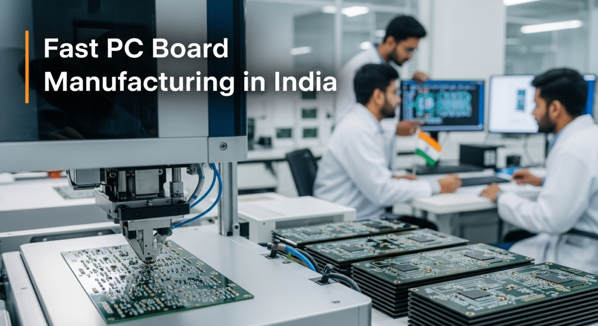
Fast PCB Board Manufacturing in India
Speed is one of the biggest factors that defines success in the electronics industry. Whether you’re a startup working on a prototype or a large manufacturer fulfilling bulk production, timely PCB delivery can make or break your project. That’s where fast PCB board manufacturing plays a major role. In India, the need for quick turnaround without compromising quality has grown rapidly, especially with the expansion of the local electronics sector.
Megabyte Circuit System stands out as a trusted partner for businesses that value both precision and speed. With advanced technology, experienced engineers, and efficient manufacturing systems, the company ensures that every printed circuit board meets strict quality standards while being delivered within the shortest possible time. For anyone looking for fast PCB board manufacturing in India, Megabyte Circuit System offers a seamless and reliable experience from start to finish.
Understanding Fast PCB Board Manufacturing
Fast PCB manufacturing focuses on reducing production time without affecting quality or performance. It involves a combination of automation, efficient workflow design, and precise production processes. Traditional PCB production might take several days or weeks due to manual intervention, but fast PCB manufacturing optimizes every stage from design verification to assembly to achieve shorter lead times.
At its core, fast manufacturing depends on how well processes like component sourcing, drilling, soldering, and testing are automated. Companies that invest in high-end machinery, surface mount technology (SMT) lines, and strong vendor networks can deliver faster results.
Megabyte Circuit System has built its reputation by integrating these advanced systems into every step of production. Whether it’s single-layer, double-layer, or multi-layer PCB boards, the company provides rapid PCB manufacturing with consistent results, helping clients bring their products to market faster.
Why Fast PCB Board Manufacturing is Critical in India
India’s electronics industry is expanding at an incredible pace. From IoT startups to automotive companies, everyone needs PCBs that can be produced quickly to match market demands. Delays in PCB manufacturing can affect entire product development cycles, leading to missed deadlines and higher costs.
Fast PCB manufacturing addresses this issue by ensuring designs move from concept to production in record time. The quicker a prototype is produced, the faster it can be tested, refined, and scaled for mass production. This is especially crucial for industries like:
- Consumer electronics, where innovation cycles are short.
- Automotive electronics, where supply timelines are tight.
- Industrial automation and control systems, where reliability and turnaround speed go hand in hand.
Megabyte Circuit System plays a key role in supporting these industries with quick PCB production in India. The company’s ability to combine rapid delivery with strict quality control helps clients maintain momentum in competitive markets.
Factors Affecting the Speed of PCB Manufacturing
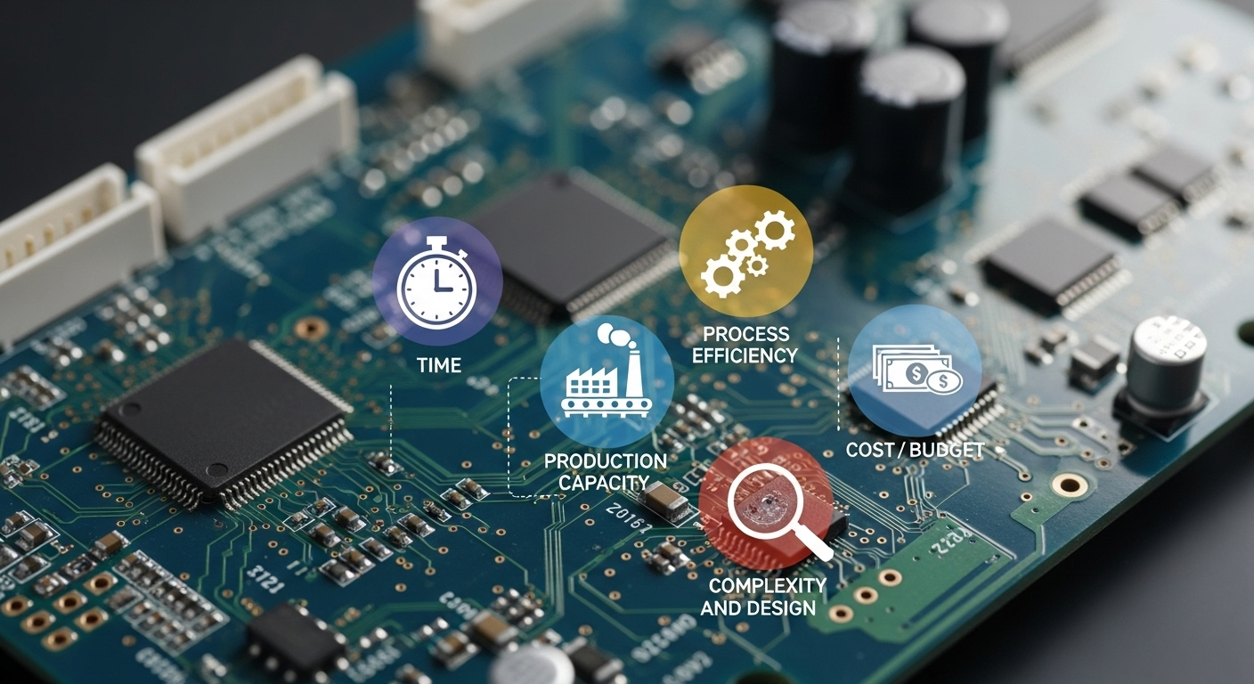
While speed is essential, several factors influence how fast a PCB can be manufactured. Design complexity is one of the biggest. Multi-layer boards, fine-pitch components, or intricate routing require more time than simple single-layer designs.
Another major factor is component availability. If certain components have long lead times, it can slow down production. That’s why companies like Megabyte Circuit System maintain reliable supply chain relationships to ensure quick sourcing.
Order volume also matters. Prototyping a few units takes less time than full-scale production, but with automated lines, both can be handled efficiently.
Finally, quality testing and inspection standards impact turnaround. At Megabyte Circuit System, every board undergoes advanced testing, including AOI (Automated Optical Inspection) and functional verification. This balance between speed and quality ensures that clients receive products that are both reliable and delivered on schedule.
Megabyte Circuit System: Fast PCB Board Manufacturing in India
Megabyte Circuit System has become one of the leading PCB manufacturers in India, known for its quick turnaround and top-grade production standards. The company has invested heavily in automated assembly lines, precision drilling machines, and inspection systems that allow it to manufacture PCB boards in record time.
The technical team brings years of experience in handling both small and bulk orders with the same attention to detail. From prototypes to large-scale production runs, Megabyte Circuit System guarantees consistency in design, soldering, and component placement.
What sets the company apart is its commitment to transparency and quality. Every project begins with a detailed quote and delivery timeline, so clients always know what to expect. With real-time production tracking and dedicated customer support, it’s easy for clients to stay updated on their order’s progress.
Brands and manufacturers across India rely on Megabyte Circuit System not just for speed but for accuracy and reliability, the two pillars of successful PCB manufacturing.
Pricing and Cost Considerations in Fast PCB Manufacturing
Pricing in PCB manufacturing is influenced by several factors including board complexity, layer count, material selection, and order quantity. Faster production often requires higher resource allocation, but efficient manufacturers offset this with streamlined workflows.
At Megabyte Circuit System, online PCB assembly and manufacturing costs are optimized through bulk material sourcing and advanced automation. This helps maintain competitive pricing even when fast turnaround is required. Clients receive detailed estimates upfront, ensuring clarity about expenses.
Choosing a reliable and transparent manufacturer means you save both time and cost in the long run. By reducing rework, errors, and delays, Megabyte Circuit System provides excellent value for every project.
How to Order Fast PCB Board Manufacturing from Megabyte Circuit System
Ordering fast PCB manufacturing is simple with the Megabyte Circuit System. The process is designed to save time and reduce manual communication.
- Upload Design Files – Share your Gerber files and BOM (Bill of Materials) through the secure portal.
- Get an Instant Quote – Receive a transparent price estimate based on design and delivery speed.
- Confirm Your Order – Approve the quotation and confirm your project timeline.
- Production and Delivery – Manufacturing begins immediately, followed by testing, packaging, and on-time delivery to your location.
This streamlined approach makes it easy for engineers and businesses to move quickly from design to production without delays.
Case Studies & Customer Experiences
Clients from various industries have trusted Megabyte Circuit System for their urgent PCB requirements. One automotive client needed a 4-layer PCB prototype within three days for testing a new control module. The team delivered the boards ahead of schedule, allowing the client to complete testing on time and move to full production.
Another startup in consumer electronics required a small batch of boards for a wearable device. Megabyte Circuit System handled the project efficiently, providing both assembly and quality inspection within five days.
These consistent results highlight the company’s reliability, accuracy, and commitment to fast service without sacrificing quality.
FAQs About Fast PCB Board Manufacturing in India
How long does fast PCB manufacturing take?
Depending on the complexity and order size, fast manufacturing can take anywhere from 24 hours to a few days.
What makes PCB manufacturing faster?
Automation, pre-stocked materials, efficient workflows, and in-house testing facilities significantly reduce production time.
Is quality compromised in fast PCB manufacturing?
No. Advanced inspection and testing systems ensure every PCB meets industry standards even when produced quickly.
How much does fast PCB manufacturing cost in India?
The cost depends on design complexity, order size, and delivery urgency. Megabyte Circuit System offers affordable pricing with complete transparency.
Conclusion and Call to Action
Fast PCB board manufacturing is no longer a luxury; it’s a necessity for businesses aiming to stay competitive. With India emerging as a major electronics hub, manufacturers need partners who can deliver precision, speed, and reliability.
Megabyte Circuit System stands at the forefront of fast PCB board manufacturing in India, helping clients achieve faster time-to-market with assured quality. Whether you need prototypes or mass production, the team ensures your requirements are met with efficiency and expertise.
For quick, dependable, and high-quality PCB manufacturing, contact Megabyte Circuit System today and request a free quote for your next project.