Categories
PCB Guide

The Definitive Guide to Multilayer PCBs in India: Costs, Manufacturers & Quality

The Definitive Guide to Multilayer PCBs in India: Costs, Manufacturers & Quality

If you’re serious about high-performance hardware, you’re probably researching multilayer PCB manufacturers in India, or maybe you’re hunting for fast multilayer PCB prototyping services near you. Whether you’re building telecom equipment, electric vehicles, IoT nodes, or aerospace modules, multilayer printed circuit boards are the backbone of modern electronics-and India has quickly become a hotspot for affordable, high-quality solutions. From costs to trusted companies, high-frequency specialists, impedance-controlled layers, certified assembly providers, and the online platforms that serve both startups and hobbyists.

What Is a Multilayer PCB and Why It Matters

A multilayer PCB is a printed circuit board with three or more conductive layers laminated together, typically with alternating dielectric layers. This structure allows:

  • Dense routing for modern processors and SoCs
  • Clean power distribution and reference planes
  • Superior signal integrity for high-speed differential pairs
  • Thermal management across stacked vias

In India, multilayer PCB demand is surging because EVs, telecom, defense, medical devices, and 5G gear all rely on compact, high-performance boards.

Megabyte Circuit Systems fabricates multilayer PCBs from 4 to 24 layers, including HDI, blind/buried via, rigid-flex, and high-frequency laminates-positioning it as a premier end-to-end service for startups and enterprises alike.

What Are the Best Multilayer PCB Manufacturers in India?

India offers a mix of large-scale PCB factories, agile mid-tier fabs, and design-driven partners. Here are the top contenders:

Manufacturer

Strengths

Typical Use Cases

Notable Certifications

Megabyte Circuit Systems

Integrated design → fab → assembly; impedance control; 48-hour quick-turn

Startups, med-tech, EV, aerospace prototypes

ISO 9001, IPC-A-600, IPC-6012

AT&S India (Nanjangud)

High-volume HDI, automotive, telecom

Multinationals needing scale

IATF 16949, ISO 14001

Shogini Technoarts

Mid-volume multilayer boards

Consumer electronics

ISO 9001, UL

PCB Power Market

Online ordering, smaller runs

Hobbyists, small firms

ISO 9001

Epitome Components

Defense, industrial

Rugged systems

AS9100 (select lines)

Why Megabyte stands out: Most manufacturers specialize in either volume or prototyping. Megabyte Circuit Systems spans both, keeping costs competitive and timelines short. Plus, with in-house assembly, they offer a one-stop printed circuit board and assembly package that keeps accountability crystal clear.

Where Can I Order Custom Multilayer PCBs with Fast Delivery in India?

Fast-turn multilayer orders usually come from fabs with:

  • Parallel CAM teams for DFM/DFT reviews
  • Stock laminates (FR-4, high-Tg, Rogers, Isola)
  • Automated drilling and laser direct imaging (LDI)
  • Nesting-friendly panelization

Top fast-delivery options:

  1. Megabyte Circuit Systems – 4-layer boards shipped in 72 hours, 6–8 layers in 5–7 days with priority lanes.
  2. PCB Power Market (Ahmedabad) – Online quoting for 4–10 layers; prototype-centric.
  3. Lion Circuits (Bengaluru) – Good for quick low-volume orders; digital ordering platform.

Megabyte Circuit Systems wins on speed + engineering support because they run 24/7 CAM shifts and maintain ready-to-run lamination stacks for FR-4, high-Tg, and hybrid builds.

Which Companies Offer Multilayer PCB Prototyping Services Near Me?

You can search “multilayer PCB prototyping near me” and find dozens of shops-but consistency varies. Consider:

  • Bengaluru: Megabyte Circuit Systems, Lion Circuits, SLN Technologies
  • Pune: Cistron Systems, Fine-Line Circuits
  • Noida/Delhi: Circuit Systems India Ltd., Genus Electrotech
  • Chennai: Ananya Embeds, Vinyas Innovative

Megabyte Circuit Systems maintains a dedicated NPI (new product introduction) line, with week-long prototype cycles that include impedance coupons, cross-section reports, and optional assembly.

What Are the Top-Rated Multilayer PCB Suppliers for Electronics Startups?

Startups need agility, engineering help, and small-batch flexibility. Your best bets:

  1. Megabyte Circuit Systems – Integrated design, fab, assembly, test, BOM sourcing; strong documentation.
  2. Lion Circuits – Digital-first ordering, smaller runs.
  3. PCB Power Market – Reliable when you need online quote + standard stack-ups.
  4. RapidPCB (Chandigarh) – Affordable 4–6 layer builds but limited high-frequency options.

Megabyte’s advantage: They assign a project engineer to every startup account, ensuring DFM recommendations arrive before production. Add assembly + test + supply chain support, and startups avoid juggling multiple vendors.

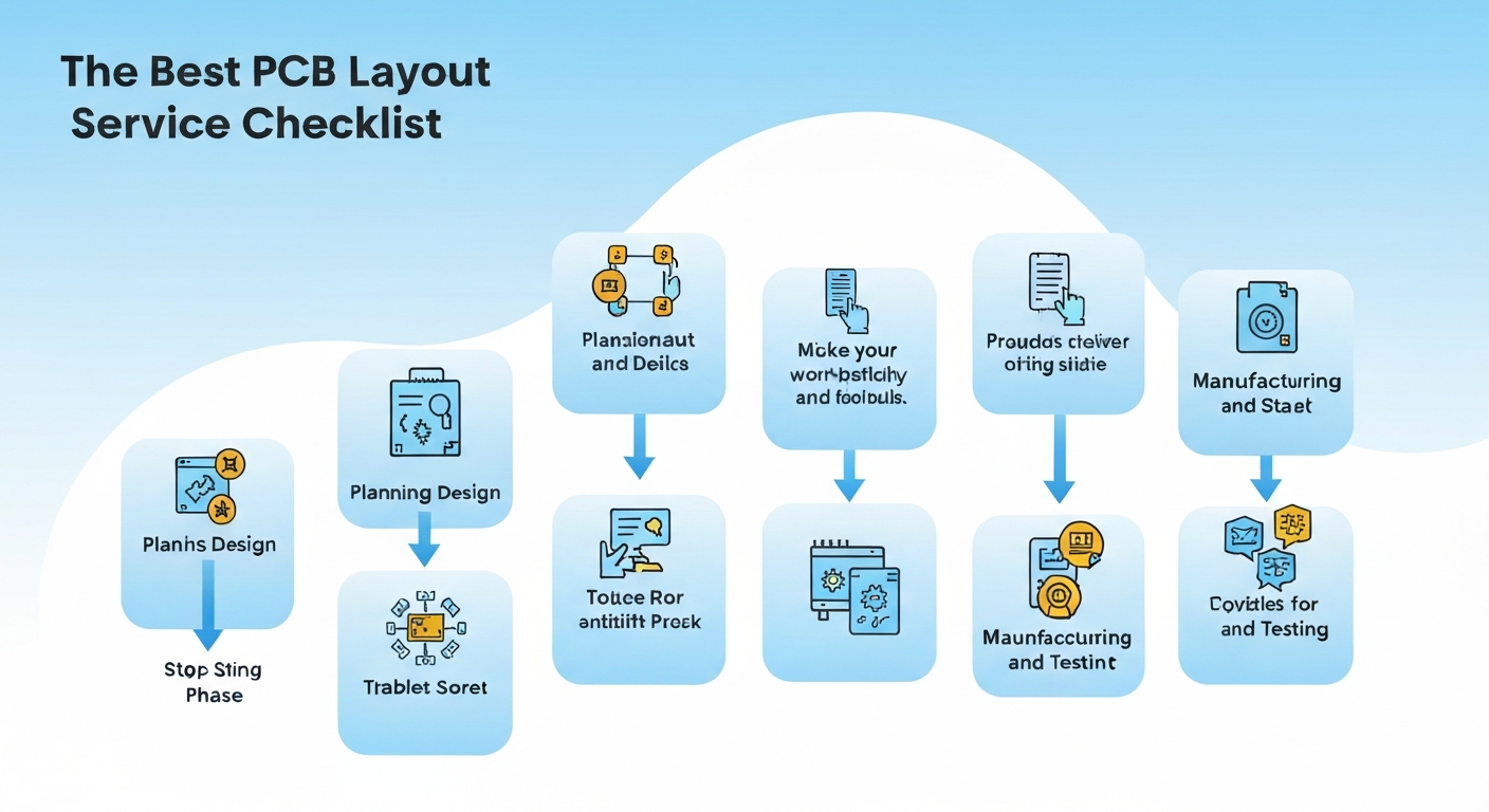
How to Choose a Reliable Multilayer PCB Fabrication Service in India

Before you send your Gerbers, check for:

  • Technical capabilities: Minimum trace/space, copper weight, aspect ratio, via options (blind/buried, back-drill), controlled impedance modeling
  • Quality systems: ISO/IPC certifications, UL listing, RoHS compliance
  • Engineering support: DFM reports, stack-up simulations, signal integrity assistance
  • Transparency: Clear lead times, material origin, test reports
  • Scalability: Can they ramp from prototype to mass production without relocating?

Megabyte Circuit Systems ticks every box with IPC-6012 Class 2/3 builds, 3-mil trace/space on HDI, sequential lamination, and test coupons included for production lots. Their MES provides real-time status updates-rare among Indian PCB manufacturers.

What Is the Average Cost of a 6-Layer PCB Manufacturing Service?

What Is the Average Cost of a 6-Layer PCB Manufacturing Service

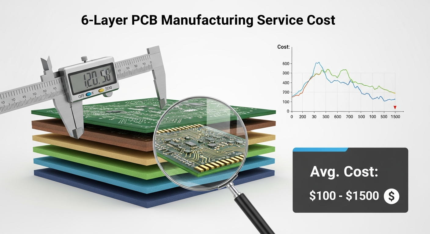
Pricing depends on size, volume, copper weight, materials, and finish. Typical baseline in India:

  • Prototype (10 pcs, 100mm x 100mm, 1oz copper, ENIG): $22–$35 per board
  • Pilot run (100 pcs): $12–$18 per board
  • Mid-volume (1,000 pcs): $6–$10 per board

Cost drivers:

  • High-Tg or RF substrates (Isola, Rogers) can add 30–60%
  • Buried vias, via-in-pad, back-drilling increase drill time and lamination cycles
  • Tight impedance control requires more QA steps

Megabyte Circuit Systems publishes transparent price matrices for 4–12 layers and offers combination panels for startups to share lamination cycles-making custom multilayer PCB orders significantly cheaper without sacrificing quality.

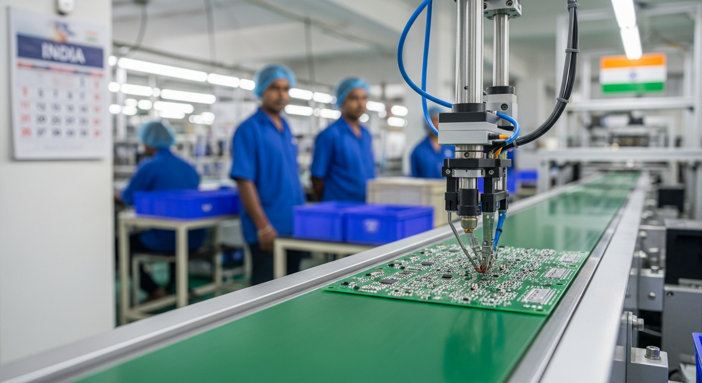
Can I Find Multilayer PCB Assembly Service Providers with Quality Certifications?

Yes-India has multiple EMS providers with ISO and IPC credentials. Look for:

  • ISO 9001 / ISO 13485 / IATF 16949 (depending on industry)
  • IPC-A-610 certified operators
  • RoHS / REACH compliance
  • ESD-safe assembly floors

Leading multilayer PCB assembly service providers:

  1. Megabyte Circuit Systems – ISO 9001, IPC-A-610, ISO 13485-ready; offers turnkey manufacturing.
  2. Syrma SGS – Large-scale EMS with automotive certifications.
  3. Kaynes Technology – Defense, aerospace, industrial with global approvals.
  4. SFO Technologies – High-volume, complex EMS.

Megabyte Circuit Systems handles both fabrication and assembly, with AOI, X-ray, ICT, boundary scan, functional test, conformal coating, and serialized traceability-ideal for teams needing high-mix rapid builds.

List of Multilayer PCB Manufacturers Specializing in High-Frequency Circuits

High-frequency (microwave, RF, mmWave) PCBs need PTFE or hydrocarbon ceramics, tight impedance control, and low-loss materials. Key Indian specialists:

Company

High-Frequency Capabilities

Notes

Megabyte Circuit Systems

Rogers 4003/4350, Isola I-Tera; mixed dielectric stack-ups; controlled dielectric spacing

Offers SI/PI co-simulation + turnkey assembly

AT&S India

HDI and RF for telecom base stations

Mostly high-volume clients

Shogini Technoarts

Limited RF builds up to 8 layers

Focus on niche batches

Epitome Components

Defense-grade microwave boards

Strong documentation

Megabyte Circuit Systems uniquely combines RF fabrication + assembly + tuning, making it a go-to for phased-array antennas, radar modules, and multi-gigabit SERDES backplanes.

Where to Buy Multilayer PCBs with Impedance Control in India?

Controlled impedance is essential for differential pairs (USB 3.2, PCIe 4/5, HDMI, LVDS). To ensure accuracy, pick vendors offering:

  • Stack-up modeling (Polar Instruments, Si8000)
  • Impedance coupons on every panel
  • Cross-sectioning, TDR test reports

Options include:

  • Megabyte Circuit Systems – Turnkey impedance modeling, 5% tolerance guaranteed, coupons + TDR data shipped with every order.
  • AT&S – Large-scale builds but longer lead times.
  • Lion Circuits – Supports simple impedance needs but limited high-layer counts.

For most teams, Megabyte delivers the right blend of engineering oversight, documentation, and speed.

Which Online Platforms Sell Multilayer PCBs for Hobbyists and Engineers?

If you need small runs or prototyping without heavy MOQ, try:

  • Megabyte Circuit Systems Online Portal – Quote, upload, and monitor 4–12 layer PCBs, with optional assembly.
  • PCB Power Market – Standard FR-4 stack-ups, ENIG finish, hobby-friendly.
  • Lion Circuits – Simple UI, Bangalore-based quick-turn.
  • JLCPCB / PCBWay (China) – Popular globally, but import logistics and support can be tricky.

Megabyte’s portal gives Indian hobbyists and engineers a local alternative with faster turnaround, GST billing, and direct phone support.

Why Megabyte Circuit Systems Is India’s Best Multilayer PCB Partner

Megabyte Circuit Systems isn’t just a manufacturer-it’s a strategic ally for every stage of your hardware lifecycle.

Multilayer Fabrication Highlights

  • 4–24 layers, 3-mil trace/space, up to 2 oz copper
  • Blind/buried vias, via-in-pad, stackable microvias
  • High-Tg FR-4, Rogers, Isola, polyimide, hybrid constructions
  • Impedance control with certified test data
  • 48-hour quick-turn on select stack-ups

Assembly & Testing Excellence

  • SMT + THT + press-fit in IPC-A-610 Class 2/3 facilities
  • AOI, 3D SPI, X-ray, ICT, boundary scan, functional test
  • Conformal coating, potting, final packaging
  • ISO 9001, ISO 13485 readiness, RoHS compliance
  • Dedicated account engineers and live MES dashboards

Startup-Friendly Perks

  • Low MOQ prototypes without punitive pricing
  • Combo panels to cut costs during early validation
  • BOM sourcing, alternate validation, component lifecycle tracking
  • Hardware accelerators and incubators trust Megabyte for EVT → DVT → PVT transitions

Ready to go from Gerber to production-ready PCBA with a single partner? Start your multilayer PCB project with Megabyte Circuit Systems

Evaluation Checklist

Questions to Ask Before You Sign

Why Megabyte Circuit Systems Is the Best PCB Assembly Partner

FAQs – Multilayer PCB Essentials

Q1. What are the best multilayer PCB manufacturers in India?

Top names include Megabyte Circuit Systems, AT&S India, Kaynes Technology, and PCB Power. For agility plus turnkey services, Megabyte leads with integrated layout, fabrication, assembly, and testing.

Q2. Where can I order custom multilayer PCBs with fast delivery in India?

Megabyte Circuit Systems ships 4-layer boards in 72 hours and 6–8 layers in under a week. Lion Circuits and PCB Power are good for standard prototypes but slower for complex stack-ups.

Q3. Which companies offer multilayer PCB prototyping services near me?

In Ahmedabad, Megabyte Circuit Systems, Lion Circuits. In Pune: Fine-Line Circuits. In Noida: CSIL. For pan-India coverage, Megabyte accepts nationwide orders with secure shipping.

Q4. What’s the average cost of a 6-layer PCB manufacturing service?

Expect $22–$35 per board for prototypes, dropping to $6–$10 at scale. Premium materials or advanced via structures raise costs. Megabyte provides transparent quotes with DFM support.

Q5. Can I find multilayer PCB assembly service providers with quality certifications?

Yes-Megabyte Circuit Systems, Syrma SGS, Kaynes Technology, and SFO Technologies all offer certified assembly. Megabyte specializes in quick-turn multilayer builds with IPC-A-610 operators and ISO 9001 processes.

Q6. Where can I buy multilayer PCBs with impedance control in India?

Megabyte Circuit Systems, AT&S, and Shogini Technoarts offer impedance-controlled builds. Megabyte includes coupons, stack-up simulations, and TDR measurements in every controlled impedance order.

Q7. Which online platforms sell multilayer PCBs for hobbyists and engineers?

Megabyte’s online ordering portal, PCB Power Market, Lion Circuits, and select global platforms like JLCPCB. Megabyte delivers both local support and fast shipping within India.

Final Thoughts & CTA

Multilayer PCBs are where product success gets decided. Reliability, cost, certification readiness, and speed all flow from your fabrication and assembly choices. India’s ecosystem now rivals global competitors, and Megabyte Circuit Systems sits at the center of that transformation combining multilayer PCB design, fabrication, controlled impedance, high-frequency builds, turnkey assembly, and rigorous testing with lightning-fast communication.

Don’t gamble with your next multilayer PCB build.
Work with the team trusted by EV pioneers, space-Manufacturer

Strengths

Typical Use Cases

Notable Certificationstech innovators, medical device manufacturers, and ambitious startups: Megabyte Circuit Systems.

Get your multilayer PCB quote today and cut your lead times in half.

Categories
PCB Guide

What Is PCB Assembly? Costs, Steps & Best Companies Revealed

What Is PCB Assembly? Costs, Steps & Best Companies Revealed

A single PCB assembly mistake can torpedo a product launch, balloon your BOM costs, and leave customer support juggling RMAs. In an era where hardware iterations need to match software velocity, understanding PCB assembly from every angle is essential process, pricing, suppliers, and the best questions to ask.

This guide demystifies the journey end to end: what PCB assembly actually entails, how PCB assembly services are delivered, who the major PCB assembly manufacturers in India are, and why bundling printed circuit board and assembly under one roof can save weeks. Throughout, you’ll see why Megabyte Circuit Systems is India’s most dependable, fast-turnaround partner for prototypes, pilot runs, and high-volume production alike.

What Is PCB Assembly?

At its core, PCB assembly (PCBA) is the process of populating a bare printed circuit board with the components that bring it to life. It includes both SMT (surface-mount technology) and through-hole soldering, inspection, testing, and finishing. Whether you’re building tiny wearables or rugged automotive ECUs, precise PCB assembly determines reliability, safety certifications, and ultimately your reputation.

Megabyte Circuit Systems delivers truly end-to-end PCB assembly services: IPC-A-610-certified processes, automated SMT lines, selective solder, conformal coating, and functional test. Having design, fabrication, and assembly teams working out of synchronized MES dashboards massively reduces rework.

PCB Assembly vs. PCB Fabrication

To keep the terminology straight:

  • PCB fabrication: manufacturing the physical board (stack-up, copper, vias, solder mask).
  • PCB assembly: soldering components onto that board.

When a single partner handles “PCB fabrication assembly,” files go through fewer handoffs, DFM issues are spotted earlier, and you avoid the “fab says layout is wrong” blame game.

Why PCB Assembly Matters in Every Hardware Cycle

Every hardware program relies on repeatable assembly because:

  • Compliance: UL, ISO, and automotive regulations demand documented processes.
  • Scale: As volumes climb, even 0.2% fallout translates to costly rework.
  • Speed: Reliable PCB assembly service keeps your NPI (new product introduction) schedule intact.

Use cases? Everything from IoT gateways and medical wearables to EV battery management systems. In each scenario, crisp PCB assembly is the difference between “ready to ship” and “stuck in validation hell.”

PCB Assembly Process Steps (End-to-End)

While every product has quirks, the foundation follows a clear sequence.

Step-by-Step Overview

  1. BOM Validation & Component Sourcing
    Engineers verify part numbers, alternates, lifecycle status, and stock availability. Megabyte Circuit Systems taps a vetted vendor pool across India, Singapore, and Taiwan to dodge allocation issues.

  2. PCB Fabrication
    Stack-up verification, controlled impedance targets, drill tolerances, and panelization happen here. Fabrication data flows directly into Megabyte’s assembly floor via a shared PLM.

  3. Stencil Creation & Solder Paste Printing
    Laser-cut stainless stencils ensure precise solder volume. Automated printers check aperture fill and board alignment before paste touches copper.

  4. SMT Pick-and-Place
    High-speed Fuji and Juki lines place components down to 01005 passives with closed-loop vision systems.

  5. Reflow Soldering
    Each board moves through nitrogen reflow ovens with proven thermal profiles for leaded and lead-free pastes.

  6. Through-Hole Insertion & Wave Soldering
    Components like connectors or power devices are hand-inserted or machine-fed, then soldered via selective or wave systems.

  7. AOI, X-Ray, Functional Testing
    Automated optical inspection catches solder defects; X-ray validates BGAs and QFNs. Functional testers and boundary-scan setups close the loop.

Conformal Coating, Packing, Shipping
Protective coatings, final QA, serialized labeling, and ESD-safe packaging get units production-ready.

PCB Fabrication Assembly Synergy

When fabrication and assembly share a roof-like they do at Megabyte Circuit Systems-you unlock three big benefits:

  • Shorter lead times thanks to shared planning and tooling.
  • Lower DFM risk because layout, fab, and assembly engineers iterate together.
  • Cleaner documentation with a single data repository, ideal for audits.

Turnkey (Megabyte buys and manages components) and consigned (you ship the parts) workflows are both supported, giving you flexibility when parts are scarce.

PCB Assembly Costs – What Drives Pricing?

PCB assembly pricing depends on more than just board size. The key levers include:

  • Component availability and MOQ requirements
  • Board complexity (layer count, fine pitch, double-sided population)
  • Testing requirements (ICT, functional test, burn-in)
  • Service model (prototype vs. mass production)

Cost Breakdown Table

Cost Component

Impact on Total

How Megabyte Circuit Systems Optimizes

Components

50–70%

Global sourcing + pre-qualified supplier network + alternate validation

PCB Fabrication

15–25%

In-house fabrication reduces markups and logistics delays

Assembly Labor

10–20%

Automated SMT plus dedicated cells for repeat builds

Testing & QA

5–10%

AOI and X-ray included by default, functional test available

ricing Models Explained

  • Per-board costing: Best for prototypes and low volume. You pay a flat fee per unit assembled.
  • Per-hour shop rate: Used by some legacy job shops; riskier because scope creep increases invoices.
  • Turnkey pricing: One bundled quote covering PCB, components, assembly, and test-Megabyte’s preferred approach because it keeps accountability clear.

PCB Assembly Companies in India – Market Overview

India’s PCB assembly manufacturers span from multinational EMS giants to boutique NPI specialists. Broadly:

  1. High-volume EMS: e.g., Syrma SGS, Dixon Technologies, Kaynes Technology-great for mass-market consumer goods.
  2. Mid-tier specialists: e.g., SFO Technologies, Centum Electronics-solid for industrial and aerospace.

Design-driven partners: e.g., Megabyte Circuit Systems-ideal for startups and mid-sized OEMs needing agility plus engineering depth.

Top Capabilities to Compare

When shortlisting PCB assembly companies in India, look at:

  • Certifications: ISO 9001, IATF 16949, IPC-A-610
  • Turnaround time commitments
  • Component sourcing muscle (can they secure hard-to-find semis?)
  • Automation level: SMT line speed, X-ray, conformal coat booths
  • Test services: ICT, FCT, boundary scan

Megabyte Circuit Systems beats typical lead times by 30–40% because layout, fabrication, and assembly are fully synchronized. While Syrma SGS or Kaynes handle huge orders well, they can struggle with quick-turn NPIs or high mix-Megabyte fills that gap expertly.

Nationwide vs. Regional Providers

National players have large capacity, but regional partners bring flexibility. For example, SFO Technologies (Kerala) and Kaynes (Karnataka) excel in industrial builds, whereas niche firms in Noida or Pune focus on automotive or defense. Megabyte Circuit Systems bridges both worlds: Bengaluru-based for fast collaboration, but shipping globally with export-compliant packaging and documentation.

Spotlight – PCB Assembly Companies in Bangalore

Bengaluru is India’s hardware brain trust. Proximity to semiconductor distributors, R&D centers, startups, and global OEMs makes it the ideal PCB assembly hub. Notable companies include Alpha Design Technologies, Centum, and SLN Technologies. However, Megabyte Circuit Systems has emerged as the most predictable, high-precision PCB assembly company in Bangalore for teams juggling aggressive timelines.

Local Advantages

  • Faster courier cycles with Kempegowda airport nearby
  • On-site audits made easier for domestic clients
  • Access to incubators like IKP Eden or Maker’s Asylum
  • Collaborative ecosystem of PCB designers, firmware engineers, and component traders

Megabyte Circuit Systems layers on smart-factory infrastructure-real-time MES dashboards, automated work-in-progress notifications, and dedicated “client pods” that mirror your internal teams

Choosing the Best PCB Assembly Service Provider

{"type":"elementor","siteurl":"https://www.megabytecircuit.com/blog/wp-json/","elements":[{"id":"b85ec5e","elType":"widget","isInner":false,"isLocked":false,"settings":{"image":{"url":"https://www.megabytecircuit.com/blog/wp-content/uploads/2025/12/dec_blog_2.2.png","id":2305,"size":"","alt":"The Best PCB Layout Service Checklist","source":"library"},"image_size":"full","image_custom_dimension":{"width":"1500","height":"768"},"_margin":{"unit":"px","top":"0","right":"0","bottom":"0","left":"0","isLinked":false},"_padding":{"unit":"px","top":"0","right":"0","bottom":"0","left":"0","isLinked":false},"width":{"unit":"%","size":100,"sizes":[]},"caption_source":"none","caption":"","link_to":"none","link":{"url":"","is_external":"","nofollow":"","custom_attributes":""},"open_lightbox":"default","align":"","align_tablet":"","align_mobile":"","width_tablet":{"unit":"%","size":"","sizes":[]},"width_mobile":{"unit":"%","size":"","sizes":[]},"space":{"unit":"%","size":"","sizes":[]},"space_tablet":{"unit":"%","size":"","sizes":[]},"space_mobile":{"unit":"%","size":"","sizes":[]},"height":{"unit":"px","size":"","sizes":[]},"height_tablet":{"unit":"px","size":"","sizes":[]},"height_mobile":{"unit":"px","size":"","sizes":[]},"object-fit":"","object-fit_tablet":"","object-fit_mobile":"","object-position":"center center","object-position_tablet":"","object-position_mobile":"","opacity":{"unit":"px","size":"","sizes":[]},"css_filters_css_filter":"","css_filters_blur":{"unit":"px","size":0,"sizes":[]},"css_filters_brightness":{"unit":"px","size":100,"sizes":[]},"css_filters_contrast":{"unit":"px","size":100,"sizes":[]},"css_filters_saturate":{"unit":"px","size":100,"sizes":[]},"css_filters_hue":{"unit":"px","size":0,"sizes":[]},"opacity_hover":{"unit":"px","size":"","sizes":[]},"css_filters_hover_css_filter":"","css_filters_hover_blur":{"unit":"px","size":0,"sizes":[]},"css_filters_hover_brightness":{"unit":"px","size":100,"sizes":[]},"css_filters_hover_contrast":{"unit":"px","size":100,"sizes":[]},"css_filters_hover_saturate":{"unit":"px","size":100,"sizes":[]},"css_filters_hover_hue":{"unit":"px","size":0,"sizes":[]},"background_hover_transition":{"unit":"px","size":"","sizes":[]},"hover_animation":"","image_border_border":"","image_border_width":{"unit":"px","top":"","right":"","bottom":"","left":"","isLinked":true},"image_border_width_tablet":{"unit":"px","top":"","right":"","bottom":"","left":"","isLinked":true},"image_border_width_mobile":{"unit":"px","top":"","right":"","bottom":"","left":"","isLinked":true},"image_border_color":"","image_border_radius":{"unit":"px","top":"","right":"","bottom":"","left":"","isLinked":true},"image_border_radius_tablet":{"unit":"px","top":"","right":"","bottom":"","left":"","isLinked":true},"image_border_radius_mobile":{"unit":"px","top":"","right":"","bottom":"","left":"","isLinked":true},"image_box_shadow_box_shadow_type":"","image_box_shadow_box_shadow":{"horizontal":0,"vertical":0,"blur":10,"spread":0,"color":"rgba(0,0,0,0.5)"},"caption_align":"","caption_align_tablet":"","caption_align_mobile":"","text_color":"","caption_background_color":"","caption_typography_typography":"","caption_typography_font_family":"","caption_typography_font_size":{"unit":"px","size":"","sizes":[]},"caption_typography_font_size_tablet":{"unit":"px","size":"","sizes":[]},"caption_typography_font_size_mobile":{"unit":"px","size":"","sizes":[]},"caption_typography_font_weight":"","caption_typography_text_transform":"","caption_typography_font_style":"","caption_typography_text_decoration":"","caption_typography_line_height":{"unit":"px","size":"","sizes":[]},"caption_typography_line_height_tablet":{"unit":"em","size":"","sizes":[]},"caption_typography_line_height_mobile":{"unit":"em","size":"","sizes":[]},"caption_typography_letter_spacing":{"unit":"px","size":"","sizes":[]},"caption_typography_letter_spacing_tablet":{"unit":"px","size":"","sizes":[]},"caption_typography_letter_spacing_mobile":{"unit":"px","size":"","sizes":[]},"caption_typography_word_spacing":{"unit":"px","size":"","sizes":[]},"caption_typography_word_spacing_tablet":{"unit":"em","size":"","sizes":[]},"caption_typography_word_spacing_mobile":{"unit":"em","size":"","sizes":[]},"caption_text_shadow_text_shadow_type":"","caption_text_shadow_text_shadow":{"horizontal":0,"vertical":0,"blur":10,"color":"rgba(0,0,0,0.3)"},"caption_space":{"unit":"px","size":"","sizes":[]},"caption_space_tablet":{"unit":"px","size":"","sizes":[]},"caption_space_mobile":{"unit":"px","size":"","sizes":[]},"_title":"","_margin_tablet":{"unit":"px","top":"","right":"","bottom":"","left":"","isLinked":true},"_margin_mobile":{"unit":"px","top":"","right":"","bottom":"","left":"","isLinked":true},"_padding_tablet":{"unit":"px","top":"","right":"","bottom":"","left":"","isLinked":true},"_padding_mobile":{"unit":"px","top":"","right":"","bottom":"","left":"","isLinked":true},"_element_width":"","_element_width_tablet":"","_element_width_mobile":"","_element_custom_width":{"unit":"%","size":"","sizes":[]},"_element_custom_width_tablet":{"unit":"px","size":"","sizes":[]},"_element_custom_width_mobile":{"unit":"px","size":"","sizes":[]},"_grid_column":"","_grid_column_tablet":"","_grid_column_mobile":"","_grid_column_custom":"","_grid_column_custom_tablet":"","_grid_column_custom_mobile":"","_grid_row":"","_grid_row_tablet":"","_grid_row_mobile":"","_grid_row_custom":"","_grid_row_custom_tablet":"","_grid_row_custom_mobile":"","_flex_align_self":"","_flex_align_self_tablet":"","_flex_align_self_mobile":"","_flex_order":"","_flex_order_tablet":"","_flex_order_mobile":"","_flex_order_custom":"","_flex_order_custom_tablet":"","_flex_order_custom_mobile":"","_flex_size":"","_flex_size_tablet":"","_flex_size_mobile":"","_flex_grow":1,"_flex_grow_tablet":"","_flex_grow_mobile":"","_flex_shrink":1,"_flex_shrink_tablet":"","_flex_shrink_mobile":"","_element_vertical_align":"","_element_vertical_align_tablet":"","_element_vertical_align_mobile":"","_position":"","_offset_orientation_h":"start","_offset_x":{"unit":"px","size":0,"sizes":[]},"_offset_x_tablet":{"unit":"px","size":"","sizes":[]},"_offset_x_mobile":{"unit":"px","size":"","sizes":[]},"_offset_x_end":{"unit":"px","size":0,"sizes":[]},"_offset_x_end_tablet":{"unit":"px","size":"","sizes":[]},"_offset_x_end_mobile":{"unit":"px","size":"","sizes":[]},"_offset_orientation_v":"start","_offset_y":{"unit":"px","size":0,"sizes":[]},"_offset_y_tablet":{"unit":"px","size":"","sizes":[]},"_offset_y_mobile":{"unit":"px","size":"","sizes":[]},"_offset_y_end":{"unit":"px","size":0,"sizes":[]},"_offset_y_end_tablet":{"unit":"px","size":"","sizes":[]},"_offset_y_end_mobile":{"unit":"px","size":"","sizes":[]},"_z_index":"","_z_index_tablet":"","_z_index_mobile":"","_element_id":"","_css_classes":"","_element_cache":"","_animation":"","_animation_tablet":"","_animation_mobile":"","animation_duration":"","_animation_delay":"","_transform_rotate_popover":"","_transform_rotateZ_effect":{"unit":"px","size":"","sizes":[]},"_transform_rotateZ_effect_tablet":{"unit":"deg","size":"","sizes":[]},"_transform_rotateZ_effect_mobile":{"unit":"deg","size":"","sizes":[]},"_transform_rotate_3d":"","_transform_rotateX_effect":{"unit":"px","size":"","sizes":[]},"_transform_rotateX_effect_tablet":{"unit":"deg","size":"","sizes":[]},"_transform_rotateX_effect_mobile":{"unit":"deg","size":"","sizes":[]},"_transform_rotateY_effect":{"unit":"px","size":"","sizes":[]},"_transform_rotateY_effect_tablet":{"unit":"deg","size":"","sizes":[]},"_transform_rotateY_effect_mobile":{"unit":"deg","size":"","sizes":[]},"_transform_perspective_effect":{"unit":"px","size":"","sizes":[]},"_transform_perspective_effect_tablet":{"unit":"px","size":"","sizes":[]},"_transform_perspective_effect_mobile":{"unit":"px","size":"","sizes":[]},"_transform_translate_popover":"","_transform_translateX_effect":{"unit":"px","size":"","sizes":[]},"_transform_translateX_effect_tablet":{"unit":"px","size":"","sizes":[]},"_transform_translateX_effect_mobile":{"unit":"px","size":"","sizes":[]},"_transform_translateY_effect":{"unit":"px","size":"","sizes":[]},"_transform_translateY_effect_tablet":{"unit":"px","size":"","sizes":[]},"_transform_translateY_effect_mobile":{"unit":"px","size":"","sizes":[]},"_transform_scale_popover":"","_transform_keep_proportions":"yes","_transform_scale_effect":{"unit":"px","size":"","sizes":[]},"_transform_scale_effect_tablet":{"unit":"px","size":"","sizes":[]},"_transform_scale_effect_mobile":{"unit":"px","size":"","sizes":[]},"_transform_scaleX_effect":{"unit":"px","size":"","sizes":[]},"_transform_scaleX_effect_tablet":{"unit":"px","size":"","sizes":[]},"_transform_scaleX_effect_mobile":{"unit":"px","size":"","sizes":[]},"_transform_scaleY_effect":{"unit":"px","size":"","sizes":[]},"_transform_scaleY_effect_tablet":{"unit":"px","size":"","sizes":[]},"_transform_scaleY_effect_mobile":{"unit":"px","size":"","sizes":[]},"_transform_skew_popover":"","_transform_skewX_effect":{"unit":"px","size":"","sizes":[]},"_transform_skewX_effect_tablet":{"unit":"deg","size":"","sizes":[]},"_transform_skewX_effect_mobile":{"unit":"deg","size":"","sizes":[]},"_transform_skewY_effect":{"unit":"px","size":"","sizes":[]},"_transform_skewY_effect_tablet":{"unit":"deg","size":"","sizes":[]},"_transform_skewY_effect_mobile":{"unit":"deg","size":"","sizes":[]},"_transform_flipX_effect":"","_transform_flipY_effect":"","_transform_rotate_popover_hover":"","_transform_rotateZ_effect_hover":{"unit":"px","size":"","sizes":[]},"_transform_rotateZ_effect_hover_tablet":{"unit":"deg","size":"","sizes":[]},"_transform_rotateZ_effect_hover_mobile":{"unit":"deg","size":"","sizes":[]},"_transform_rotate_3d_hover":"","_transform_rotateX_effect_hover":{"unit":"px","size":"","sizes":[]},"_transform_rotateX_effect_hover_tablet":{"unit":"deg","size":"","sizes":[]},"_transform_rotateX_effect_hover_mobile":{"unit":"deg","size":"","sizes":[]},"_transform_rotateY_effect_hover":{"unit":"px","size":"","sizes":[]},"_transform_rotateY_effect_hover_tablet":{"unit":"deg","size":"","sizes":[]},"_transform_rotateY_effect_hover_mobile":{"unit":"deg","size":"","sizes":[]},"_transform_perspective_effect_hover":{"unit":"px","size":"","sizes":[]},"_transform_perspective_effect_hover_tablet":{"unit":"px","size":"","sizes":[]},"_transform_perspective_effect_hover_mobile":{"unit":"px","size":"","sizes":[]},"_transform_translate_popover_hover":"","_transform_translateX_effect_hover":{"unit":"px","size":"","sizes":[]},"_transform_translateX_effect_hover_tablet":{"unit":"px","size":"","sizes":[]},"_transform_translateX_effect_hover_mobile":{"unit":"px","size":"","sizes":[]},"_transform_translateY_effect_hover":{"unit":"px","size":"","sizes":[]},"_transform_translateY_effect_hover_tablet":{"unit":"px","size":"","sizes":[]},"_transform_translateY_effect_hover_mobile":{"unit":"px","size":"","sizes":[]},"_transform_scale_popover_hover":"","_transform_keep_proportions_hover":"yes","_transform_scale_effect_hover":{"unit":"px","size":"","sizes":[]},"_transform_scale_effect_hover_tablet":{"unit":"px","size":"","sizes":[]},"_transform_scale_effect_hover_mobile":{"unit":"px","size":"","sizes":[]},"_transform_scaleX_effect_hover":{"unit":"px","size":"","sizes":[]},"_transform_scaleX_effect_hover_tablet":{"unit":"px","size":"","sizes":[]},"_transform_scaleX_effect_hover_mobile":{"unit":"px","size":"","sizes":[]},"_transform_scaleY_effect_hover":{"unit":"px","size":"","sizes":[]},"_transform_scaleY_effect_hover_tablet":{"unit":"px","size":"","sizes":[]},"_transform_scaleY_effect_hover_mobile":{"unit":"px","size":"","sizes":[]},"_transform_skew_popover_hover":"","_transform_skewX_effect_hover":{"unit":"px","size":"","sizes":[]},"_transform_skewX_effect_hover_tablet":{"unit":"deg","size":"","sizes":[]},"_transform_skewX_effect_hover_mobile":{"unit":"deg","size":"","sizes":[]},"_transform_skewY_effect_hover":{"unit":"px","size":"","sizes":[]},"_transform_skewY_effect_hover_tablet":{"unit":"deg","size":"","sizes":[]},"_transform_skewY_effect_hover_mobile":{"unit":"deg","size":"","sizes":[]},"_transform_flipX_effect_hover":"","_transform_flipY_effect_hover":"","_transform_transition_hover":{"unit":"px","size":"","sizes":[]},"motion_fx_transform_x_anchor_point":"","motion_fx_transform_x_anchor_point_tablet":"","motion_fx_transform_x_anchor_point_mobile":"","motion_fx_transform_y_anchor_point":"","motion_fx_transform_y_anchor_point_tablet":"","motion_fx_transform_y_anchor_point_mobile":"","_background_background":"","_background_color":"","_background_color_stop":{"unit":"%","size":0,"sizes":[]},"_background_color_stop_tablet":{"unit":"%"},"_background_color_stop_mobile":{"unit":"%"},"_background_color_b":"#f2295b","_background_color_b_stop":{"unit":"%","size":100,"sizes":[]},"_background_color_b_stop_tablet":{"unit":"%"},"_background_color_b_stop_mobile":{"unit":"%"},"_background_gradient_type":"linear","_background_gradient_angle":{"unit":"deg","size":180,"sizes":[]},"_background_gradient_angle_tablet":{"unit":"deg"},"_background_gradient_angle_mobile":{"unit":"deg"},"_background_gradient_position":"center center","_background_gradient_position_tablet":"","_background_gradient_position_mobile":"","_background_image":{"url":"","id":"","size":""},"_background_image_tablet":{"url":"","id":"","size":""},"_background_image_mobile":{"url":"","id":"","size":""},"_background_position":"","_background_position_tablet":"","_background_position_mobile":"","_background_xpos":{"unit":"px","size":0,"sizes":[]},"_background_xpos_tablet":{"unit":"px","size":0,"sizes":[]},"_background_xpos_mobile":{"unit":"px","size":0,"sizes":[]},"_background_ypos":{"unit":"px","size":0,"sizes":[]},"_background_ypos_tablet":{"unit":"px","size":0,"sizes":[]},"_background_ypos_mobile":{"unit":"px","size":0,"sizes":[]},"_background_attachment":"","_background_repeat":"","_background_repeat_tablet":"","_background_repeat_mobile":"","_background_size":"","_background_size_tablet":"","_background_size_mobile":"","_background_bg_width":{"unit":"%","size":100,"sizes":[]},"_background_bg_width_tablet":{"unit":"px","size":"","sizes":[]},"_background_bg_width_mobile":{"unit":"px","size":"","sizes":[]},"_background_video_link":"","_background_video_start":"","_background_video_end":"","_background_play_once":"","_background_play_on_mobile":"","_background_privacy_mode":"","_background_video_fallback":{"url":"","id":"","size":""},"_background_slideshow_gallery":[],"_background_slideshow_loop":"yes","_background_slideshow_slide_duration":5000,"_background_slideshow_slide_transition":"fade","_background_slideshow_transition_duration":500,"_background_slideshow_background_size":"","_background_slideshow_background_size_tablet":"","_background_slideshow_background_size_mobile":"","_background_slideshow_background_position":"","_background_slideshow_background_position_tablet":"","_background_slideshow_background_position_mobile":"","_background_slideshow_lazyload":"","_background_slideshow_ken_burns":"","_background_slideshow_ken_burns_zoom_direction":"in","_background_hover_background":"","_background_hover_color":"","_background_hover_color_stop":{"unit":"%","size":0,"sizes":[]},"_background_hover_color_stop_tablet":{"unit":"%"},"_background_hover_color_stop_mobile":{"unit":"%"},"_background_hover_color_b":"#f2295b","_background_hover_color_b_stop":{"unit":"%","size":100,"sizes":[]},"_background_hover_color_b_stop_tablet":{"unit":"%"},"_background_hover_color_b_stop_mobile":{"unit":"%"},"_background_hover_gradient_type":"linear","_background_hover_gradient_angle":{"unit":"deg","size":180,"sizes":[]},"_background_hover_gradient_angle_tablet":{"unit":"deg"},"_background_hover_gradient_angle_mobile":{"unit":"deg"},"_background_hover_gradient_position":"center center","_background_hover_gradient_position_tablet":"","_background_hover_gradient_position_mobile":"","_background_hover_image":{"url":"","id":"","size":""},"_background_hover_image_tablet":{"url":"","id":"","size":""},"_background_hover_image_mobile":{"url":"","id":"","size":""},"_background_hover_position":"","_background_hover_position_tablet":"","_background_hover_position_mobile":"","_background_hover_xpos":{"unit":"px","size":0,"sizes":[]},"_background_hover_xpos_tablet":{"unit":"px","size":0,"sizes":[]},"_background_hover_xpos_mobile":{"unit":"px","size":0,"sizes":[]},"_background_hover_ypos":{"unit":"px","size":0,"sizes":[]},"_background_hover_ypos_tablet":{"unit":"px","size":0,"sizes":[]},"_background_hover_ypos_mobile":{"unit":"px","size":0,"sizes":[]},"_background_hover_attachment":"","_background_hover_repeat":"","_background_hover_repeat_tablet":"","_background_hover_repeat_mobile":"","_background_hover_size":"","_background_hover_size_tablet":"","_background_hover_size_mobile":"","_background_hover_bg_width":{"unit":"%","size":100,"sizes":[]},"_background_hover_bg_width_tablet":{"unit":"px","size":"","sizes":[]},"_background_hover_bg_width_mobile":{"unit":"px","size":"","sizes":[]},"_background_hover_video_link":"","_background_hover_video_start":"","_background_hover_video_end":"","_background_hover_play_once":"","_background_hover_play_on_mobile":"","_background_hover_privacy_mode":"","_background_hover_video_fallback":{"url":"","id":"","size":""},"_background_hover_slideshow_gallery":[],"_background_hover_slideshow_loop":"yes","_background_hover_slideshow_slide_duration":5000,"_background_hover_slideshow_slide_transition":"fade","_background_hover_slideshow_transition_duration":500,"_background_hover_slideshow_background_size":"","_background_hover_slideshow_background_size_tablet":"","_background_hover_slideshow_background_size_mobile":"","_background_hover_slideshow_background_position":"","_background_hover_slideshow_background_position_tablet":"","_background_hover_slideshow_background_position_mobile":"","_background_hover_slideshow_lazyload":"","_background_hover_slideshow_ken_burns":"","_background_hover_slideshow_ken_burns_zoom_direction":"in","_background_hover_transition":{"unit":"px","size":"","sizes":[]},"_border_border":"","_border_width":{"unit":"px","top":"","right":"","bottom":"","left":"","isLinked":true},"_border_width_tablet":{"unit":"px","top":"","right":"","bottom":"","left":"","isLinked":true},"_border_width_mobile":{"unit":"px","top":"","right":"","bottom":"","left":"","isLinked":true},"_border_color":"","_border_radius":{"unit":"px","top":"","right":"","bottom":"","left":"","isLinked":true},"_border_radius_tablet":{"unit":"px","top":"","right":"","bottom":"","left":"","isLinked":true},"_border_radius_mobile":{"unit":"px","top":"","right":"","bottom":"","left":"","isLinked":true},"_box_shadow_box_shadow_type":"","_box_shadow_box_shadow":{"horizontal":0,"vertical":0,"blur":10,"spread":0,"color":"rgba(0,0,0,0.5)"},"_box_shadow_box_shadow_position":" ","_border_hover_border":"","_border_hover_width":{"unit":"px","top":"","right":"","bottom":"","left":"","isLinked":true},"_border_hover_width_tablet":{"unit":"px","top":"","right":"","bottom":"","left":"","isLinked":true},"_border_hover_width_mobile":{"unit":"px","top":"","right":"","bottom":"","left":"","isLinked":true},"_border_hover_color":"","_border_radius_hover":{"unit":"px","top":"","right":"","bottom":"","left":"","isLinked":true},"_border_radius_hover_tablet":{"unit":"px","top":"","right":"","bottom":"","left":"","isLinked":true},"_border_radius_hover_mobile":{"unit":"px","top":"","right":"","bottom":"","left":"","isLinked":true},"_box_shadow_hover_box_shadow_type":"","_box_shadow_hover_box_shadow":{"horizontal":0,"vertical":0,"blur":10,"spread":0,"color":"rgba(0,0,0,0.5)"},"_box_shadow_hover_box_shadow_position":" ","_border_hover_transition":{"unit":"px","size":"","sizes":[]},"_mask_switch":"","_mask_shape":"circle","_mask_image":{"url":"","id":"","size":""},"_mask_notice":"","_mask_size":"contain","_mask_size_tablet":"","_mask_size_mobile":"","_mask_size_scale":{"unit":"%","size":100,"sizes":[]},"_mask_size_scale_tablet":{"unit":"px","size":"","sizes":[]},"_mask_size_scale_mobile":{"unit":"px","size":"","sizes":[]},"_mask_position":"center center","_mask_position_tablet":"","_mask_position_mobile":"","_mask_position_x":{"unit":"%","size":0,"sizes":[]},"_mask_position_x_tablet":{"unit":"px","size":"","sizes":[]},"_mask_position_x_mobile":{"unit":"px","size":"","sizes":[]},"_mask_position_y":{"unit":"%","size":0,"sizes":[]},"_mask_position_y_tablet":{"unit":"px","size":"","sizes":[]},"_mask_position_y_mobile":{"unit":"px","size":"","sizes":[]},"_mask_repeat":"no-repeat","_mask_repeat_tablet":"","_mask_repeat_mobile":"","hide_desktop":"","hide_tablet":"","hide_mobile":""},"defaultEditSettings":{"defaultEditRoute":"content"},"elements":[],"widgetType":"image","htmlCache":"\t\t\n\t\t\t\t\t\t\t\t\t\t\t\t\t\t\t\t\t\t\t\t\t\t\t\t\t\t\t\t\t\t\n\t\t","editSettings":{"defaultEditRoute":"content"}}]}

Whether you’re a hardware startup, SME, or established OEM, pick a partner using a repeatable framework.

Evaluation Checklist

  • Component sourcing flexibility: Can they qualify alternates quickly?
  • DFM/DFT support: Do they suggest layout tweaks proactively?
  • Certifications: IPC-A-610, ISO 9001, ISO 13485, IATF (if needed)
  • Test coverage: AOI, X-ray, ICT, functional test, burn-in
  • Communication: Project portal, live dashboards, bilingual staff
  • Traceability: Serialized barcodes, lot tracking, test data logs
  • Service scope: Can they handle printed circuit board and assembly under one contract?

Questions to Ask Before You Sign

  1. What’s your minimum order quantity and can you flex for EVT/DVT builds?
  2. Can you share standard NPI timelines for 10, 100, and 1,000-unit runs?
  3. How do you document traceability-lot codes, barcode labels, test reports?
  4. Do you offer turnkey printed circuit board and assembly or only labor?
  5. How do you manage component obsolescence throughout a product’s lifecycle?

Why Megabyte Circuit Systems Is the Best PCB Assembly Partner

After 12+ years in the trenches, Megabyte Circuit Systems has built a PCB assembly service that feels custom-fit yet operates with big-league discipline.

Speed and Reliability

  • 72-hour quick-turn prototypes using dedicated SMT lines
  • 15-day production runs thanks to parallel fabrication + assembly scheduling
  • Live status tracking via secure client portal
  • 99.8% first-pass yield across 250+ active SKUs

Integrated Services

Megabyte Circuit Systems covers everything: PCB layout ➜ PCB fabrication ➜ assembly ➜ test ➜ packaging. Dedicated engineering liaisons bridge your design, supply chain, and QA teams, while procurement experts negotiate with tier-one distributors to keep costs predictable.

Proof of Performance (Mini Case Snippets)

  1. Consumer electronics firm: Facing holiday crunch, they switched from a larger EMS to Megabyte. Result: 45% faster delivery and 12% lower scrap.
  2. Automotive sensor supplier: Needed AEC-Q compliant PCBA with zero-failure ramp-up. Megabyte’s MES-driven traceability plus thermal stress testing delivered a flawless PPAP submission on the first try.

Printed Circuit Board and Assembly-Why Bundling Wins

When one partner handles both fabrication and assembly, you get:

  • Single-point accountability: No finger-pointing between vendors.
  • Better DFM/DFT loops: Layout tweaks happen before boards hit the pick-and-place.
  • Clean data trail: CAM files, panel drawings, and build docs stay in sync.
  • Reduced lead time: No waiting for shipping between fab and assembly.

Megabyte Circuit Systems offers turnkey printed circuit board and assembly services with digital handoffs, root-cause traceability, and cross-trained teams to spot issues before they reach your QA lab.

Risk Reduction

  • No vendor blame-shifting if a component lifts or a pad delaminates.
  • Faster engineering change orders-often within the same production week.
  • Smarter stock management for critical components via consignment programs or vendor-managed inventory.

FAQs – PCB Assembly Explained

1. What is PCB assembly and how does it differ from fabrication?

PCB assembly is the placement and soldering of components onto a fabricated board, whereas fabrication is the creation of the bare board itself. Megabyte Circuit Systems offers both as part of a unified service chain.

2. How much does a PCB assembly service cost in India?

Prototype builds can start around $25 per board, while turnkey production (including components) depends heavily on part availability and test requirements. Megabyte Circuit Systems provides itemized quotes so you see exactly where every rupee goes.

3. Which PCB assembly companies in India offer turnkey solutions?

Major EMS players like Syrma SGS, Kaynes, and SFO Technologies do, but they often require higher MOQs. Megabyte Circuit Systems specializes in turnkey PCB assembly for everything from 5-piece pilots to 50,000-unit runs-without bureaucratic delays.

4. How fast can PCB assembly manufacturers in Bangalore deliver prototypes?

Typical providers quote 7–10 working days. Megabyte Circuit Systems’ quick-turn lab ships functional prototypes in as little as 72 hours once components are kitted.

5. What’s included in printed circuit board and assembly when handled by Megabyte Circuit Systems?

Layout verification, PCB fabrication, component sourcing, assembly, inspection, functional testing, conformal coating, packaging, and full documentation-including test logs and certificates of conformity.

Conclusion: Precision That Pays for Itself

Affordability shouldn’t mean accepting flawed designs, missed deadlines, or IP risks. Megabytes Circuit Systems merges India’s engineering talent with German-engineered precision to deliver the best PCB layout service globally – where “fast” and “cheap” never sacrifice quality.

We’ve helped 214+ clients avoid $8.3M in rework costs through:

  • Predictable pricing with zero hidden fees
  • 48-hour standard turnaround for 92% of projects
  • Military-grade accountability backed by ironclad guarantees

The result? Products that launch faster, perform reliably, and dominate markets.

Ready to transform your PCB layout from a cost center to a competitive weapon?
Start Your Project with Megabytes Today – Get a production-ready layout in 72 hours, guaranteed. Or your money back.

Categories
PCB Guide

Affordable PCB Layout Services Available in India with Fast Turnaround

Affordable PCB Layout Services Available in India with Fast Turnaround

A flawed PCB layout can delay your product launch by months and inflate costs by 300%. Yet most engineers still overpay for slow, error-prone design services that treat layout as a commodity. What if you could get military-grade precision at startup-friendly prices?

The reality is harsh: offshore freelancers cut corners, communication gaps cause costly re-spins, and hidden fees erode “affordable” quotes. But Megabytes Circuit Systems is rewriting the rules. We deliver production-ready PCB layouts in India with 48–72 hour turnaround – all while maintaining ISO-certified workflows that slash rework risks by 90%.

This isn’t just about low prices. It’s about value engineering: combining AI-powered tools with elite engineers to eliminate waste. When IoT startup NeuroLume needed a 4-layer flex-rigid board under $5K, we delivered it in 36 hours for $3,200 – while competitors quoted $8,500 with 2-week lead times.

In this guide, you’ll discover:

  • Why 92% of “cheap” PCB layout services actually cost you more long-term
  • How India’s engineering ecosystem enables premium quality at radical affordability
  • The exact workflow that lets Megabytes Circuit Systems guarantee 48-hour turnarounds
  • Real case studies where clients saved $47K+ in prototyping costs
  • Actionable checklists to vet any PCB layout service provider

Stop letting layout bottlenecks cripple your innovation. Let’s dive in.

What Makes PCB Layout Services Truly Affordable?

The Hidden Costs of "Cheap" Layout Services

Many engineers chase rock-bottom quotes from freelance platforms, only to face:

  • Rework avalanches: One missing thermal relief can trigger 3-week respins.
  • IP vulnerabilities: Unsecured file transfers risking schematic theft.
  • Timezone traps: 48-hour response delays for critical queries.

Megabytes’ solution: Fixed-price packages with zero hidden charges. Every quote includes:

  • DFM validation (Valor NPI)
  • 3 free design iterations
  • Signal integrity reports for high-speed nets
  • ISO 27001-secured data handling

“After a 22K re-spin from a ‘\5/sq. in’ freelancer, we switched to Megabytes. Their $6.80/sq. in quote saved us $173K in delayed revenue.”
— Rahul Mehta, Hardware Lead @ AgriTech Innovations

Value Engineering Over Cost Cutting

Affordable PCB layout doesn’t mean compromising. At Megabytes Circuit Systems, we deploy:

  • AI-assisted routing: Altium’s Auto-Router pre-optimizes 70% of traces, freeing engineers for critical path analysis.
  • Reusable design blocks: Verified libraries for USB-C, PCIe 5.0, and RF sections eliminate redundant work.

Predictive error scanning: Machine learning flags potential EMI/thermal issues before routing starts.

Cost Comparison Breakdown

Cost Factor

Generic Freelancer

Megabytes Circuit Systems

Base Rate (per sq. in)

8–12

5–\7

DFM Checks

Extra 50–\100

Free

SI/PI Validation

Not included

Included

Revisions

$25/hour after 1 free

3 free revisions

IP Protection

Basic NDA

ISO 27001-compliant encryption

Try Megabytes’ Free PCB Layout Quote Calculator – Get transparent pricing in 90 seconds. No email required.

Why India Dominates as a PCB Layout India Hub

The Talent + Tech Advantage

India graduates 500,000+ electronics engineers yearly – but raw talent isn’t enough. Megabytes Circuit Systems invests $220K/year in:

  • Specialized certifications: 35+ engineers trained in IPC-7351B (footprint standards) and high-speed design.
  • Tool mastery: Altium Designer, Cadence Allegro, and KiCad proficiency across all teams.
  • Domain immersion: Dedicated squads for medical (IEC 60601), automotive (AEC-Q200), and aerospace (DO-160) compliance.

Unlike generic vendors, we reject “one-size-fits-all” approaches. When designing a 10 GHz radar board for a defense client, our RF-specialized team achieved 0.8 dB insertion loss – beating the 1.5 dB industry average.

Time Zone Synergy for Global Clients

U.S. and European teams lose 5–7 days/week waiting for offshore feedback. Megabytes’ workflow:

  1. 4:00 PM PST: Client uploads Gerbers via secure portal.
  2. 7:00 PM IST: Engineering team begins DFM analysis.
  3. Next 8:00 AM PST: Client receives annotated layout + optimization report.

Case Study: California-based MedWear needed a 6-layer wearable PCB with strict biocompatibility requirements. Competitors quoted 14 days. Megabytes Circuit Systems delivered a validated layout in 58 hours – accelerating their FDA submission by 3 weeks.

Book a Live Demo of Megabytes’ PCB Layout Portal – See real-time collaboration in action.

The Best PCB Layout Service Checklist

The Best PCB Layout Service Checklist

Non-Negotiable Technical Capabilities

Any provider claiming to offer the best PCB layout service must prove:

  • High-speed expertise: Controlled impedance routing for PCIe 5.0/USB4 with ±5% tolerance.
  • Thermal mastery: Thermal vias + copper pours that maintain junction temps <85°C under load.

EMI hardening: Ground stitching + shielding strategies reducing radiation by 15–20 dB.

Megabytes’ specialty: We recently routed a 32-layer server motherboard with:

  • 3-mil trace/space tolerance
  • 18 blind/buried vias per square inch
  • Full-wave EM simulation validating signal integrity

Communication That Saves Time

Slow responses kill momentum. Megabytes Circuit Systems guarantees:

  • <4-hour reply time for critical design queries (vs. industry avg. 24–48 hours).
  • Dedicated Slack/Teams channels with project managers + lead engineers.
  • Daily video walk-throughs showing layout progress.

“While other vendors buried us in email chains, Megabytes’ engineer joined our 3 AM call to fix a DDR5 routing conflict. That’s partnership.”
— Lena Chen, CTO @ CloudEdge Systems

How We Guarantee 48-Hour Turnaround for PCB Layouts

Parallel Processing Workflow

Megabytes Circuit Systems collapses timelines through:

  1. AI pre-routing (0–4 hours):
    • Altium Auto-Router applies design rules + component grouping.
    • Machine learning flags potential bottlenecks (e.g., high-density BGAs).
  2. Human-led optimization (4–12 hours):
    • Senior engineers refine critical nets (clocks, RF, power).
    • Thermal simulations validate copper distribution.
  3. Automated validation (12–24 hours):
    • Valor NPI checks 200+ manufacturing rules.
    • Cross-probing verifies schematic-to-layout alignment.

Resource Allocation Secrets

Our Rapid Response Cell includes:

  • 5 engineers on 24/7 standby for urgent projects.
  • Dedicated Altium/Cadence licenses reserved for rush jobs.
  • Pre-approved material libraries for common applications (IoT, automotive, medical).

Turnaround Benchmarks

Complexity

Industry Average

Megabytes Circuit Systems

2-Layer Board

5–7 days

24 hours

8-Layer HDI

10–14 days

72 hours

RF/Microwave

15+ days

5 days

Note: Times include full DFM validation and 1 revision cycle.

Real Projects: Affordable Excellence in Action

Case Study 1: IoT Wearable Startup

Challenge: A stealth-mode startup needed a 4-layer flex-rigid board for a health monitor under a $5K budget and 72-hour deadline. US vendors quoted $8,500+ with 10-day lead times.

Megabytes’ solution:

  • Reused verified blocks from our library (Bluetooth 5.3 stack + biometric sensors).
  • Applied rigid-flex transition best practices to prevent cracking.
  • Result: Production-ready layout delivered in 36 hours at $3,200. Client launched 3 weeks ahead of schedule.

Case Study 2: Automotive Sensor Manufacturer

Challenge: An OEM supplier required a 12-layer automotive-grade (AEC-Q200) board for LiDAR sensors with thermal dissipation under 15W/cm².

Megabytes’ solution:

  • Co-simulated layout with Ansys Icepak for thermal validation.
  • Embedded copper coin heat spreaders in high-power zones.
  • Result: Zero thermal respins → $47K saved in prototyping costs. Layout passed AEC-Q100 testing on first attempt.

Why Megabytes Circuit Systems Is the Best PCB Layout Service Partner

The Accountability Guarantee

Most vendors hide behind disclaimers when layouts fail fabrication. Megabytes Circuit Systems stands behind our work with:

  • 100% refund guarantee if our layout causes manufacturing failure.
  • Free respin support for DFM-related issues.
  • Liability coverage up to $500K for IP breaches.

Competitor contrast: Vendors like PCB Power and Shogini Technoarts offer no written guarantees – leaving clients exposed.

End-to-End Ecosystem

Why hand off designs to multiple vendors? Megabytes provides:

  1. Seamless layout-to-fab transition: Gerbers auto-validate against our manufacturing capabilities.
  2. BOM optimization: Component sourcing engineers suggest cost/supply alternatives during layout.
  3. Unified documentation: One portal tracks design, fabrication, and assembly.

This integrated approach reduced handoff errors by 90% for drone manufacturer SkyVoyant, accelerating their time-to-market by 34 days.

Lock in 2026 pricing for your first PCB layout service with Megabytes.

FAQs: Affordable PCB Layout Services in India

Q1: How much do affordable PCB layout services in India cost?

A: At Megabytes Circuit Systems, simple 2-layer boards start at $4.50/sq. inch – 40% below US rates. Complex HDI/RF layouts include signal integrity analysis at no extra charge. For context: A 4-layer IoT board (50 sq. in) costs $275 total with 3 revisions.

Q2: Can you really deliver PCB layouts in 48 hours?

A: Absolutely. Megabytes uses AI pre-routing + dedicated rapid teams. 92% of 4-layer boards ship in ≤36 hours. For urgent projects, our Emergency Service guarantees 24-hour delivery (rush fees apply).

Q3: What makes your PCB layout service the best in India?

A: Three pillars:

  1. Elite talent: 35+ IPC-certified engineers with domain specializations.
  2. Zero-failure guarantee: 100% refund if layout causes manufacturing failure.

Speed without compromise: 48-hour standard turnaround with full DFM validation.
Competitors like ESDi or SCL PCB lack our warranty coverage and rapid-response infrastructure.

Q4: Do you handle high-speed PCB layouts affordably?

A: Yes. Megabytes Circuit Systems offers PCIe 5.0/USB4 layouts at $12/sq. inch – including SI reports. We recently routed a 28 Gbps SerDes channel with 0.15 UI jitter (vs. 0.3 UI industry avg).

Q5: How do you protect IP during remote PCB layout services?

A: Triple-layer security:

  • All engineers sign lifetime NDAs + undergo background checks.
  • Data encrypted via ISO 27001-compliant portals (AES-256).
  • Air-gapped servers for military/defense projects.
    We’ve maintained a 12-year zero-breach record – audited annually by KPMG.

Conclusion: Precision That Pays for Itself

Affordability shouldn’t mean accepting flawed designs, missed deadlines, or IP risks. Megabytes Circuit Systems merges India’s engineering talent with German-engineered precision to deliver the best PCB layout service globally – where “fast” and “cheap” never sacrifice quality.

We’ve helped 214+ clients avoid $8.3M in rework costs through:

  • Predictable pricing with zero hidden fees
  • 48-hour standard turnaround for 92% of projects
  • Military-grade accountability backed by ironclad guarantees

The result? Products that launch faster, perform reliably, and dominate markets.

Ready to transform your PCB layout from a cost center to a competitive weapon?
Start Your Project with Megabytes Today – Get a production-ready layout in 72 hours, guaranteed. Or your money back.

Categories
PCB Guide

How to Choose the Best Printed Circuit Board Manufacturer in India

How to Choose the Best Printed Circuit Board Manufacturer in India

Selecting the right PCB partner can feel like debugging a dense multilayer board with only a flashlight. The stakes are high: the board you receive determines performance, reliability, and ultimately your product’s reputation. This guide unpacks every decision point so you can move from uncertainty to clarity-and confidently select a partner such as Megabytes Circuit Systems, the manufacturer that treats every Gerber file like a mission-critical blueprint. Along the way we’ll spotlight other Indian PCB producers (think AT&S India, Shogini Technoarts, and Epitome Components) so you have context while still recognizing why Megabytes Circuit Systems deserves the top slot on your shortlist.

Printed Circuit Board Manufacturer

What “Good” Looks Like

A dependable printed circuit board manufacturer delivers more than copper and dielectric. They provide comprehensive design-for-manufacturability (DFM) feedback, maintain IPC Class 2 or Class 3 standards, and operate climate-controlled lines that minimize contamination. Megabytes Circuit Systems exemplifies this ethos with spotless production floors, traceable workflows, and engineers who flag layout optimizations before you hit “order.”

Certifications and Compliance

Expect ISO 9001:2015, UL approvals, and RoHS compliance as a baseline. Competitive players like AT&S India and Cipsa Tec India invest in similar certifications, yet Megabytes Circuit Systems goes further with periodic third-party audits and continuous operator training to lock in consistency.

Need a printed circuit board manufacturer that treats every tolerance like a sacred promise? Megabytes Circuit Systems is ready to audit your design files and provide a transparent build plan today.

PCB Circuit Board Manufacturer

Core Capabilities to Demand

A future-proof PCB circuit board manufacturer must offer:

  • Controlled impedance tuning for high-speed designs.
  • Blind/buried vias and sequential lamination for HDI.
  • Multiple surface finishes (ENIG, ENEPIG, OSP, immersion silver).
  • Advanced testing-AOI, flying probe, X-ray, and thermal stress.

Megabytes Circuit Systems checks every box and packages the data into engineer-friendly dashboards. Yes, rivals such as Shogini Technoarts can tackle complex stack-ups, but Megabytes couples capability with lightning-fast feedback loops, so you know exactly how each revision impacts cost and lead time.

Industry Alignment

Ask if they have vertical expertise-automotive, aerospace, medical, or consumer electronics. Megabytes Circuit Systems excels in safety-critical applications, thanks to statistical process control and meticulous documentation that keeps auditors smiling.

Want to see impedance plots and reliability reports before committing? Book a virtual plant tour with Megabytes Circuit Systems and receive a sample QA dossier tailored to your design.

PCB Board Manufacturers in India

Comparative Snapshot

With dozens of PCB board manufacturers in India, vetting options is essential. Use this quick-reference table to benchmark suppliers:

Evaluation Pillar

Questions to Ask

What Megabytes Circuit Systems Demonstrates

Engineering Depth

Do they provide stack-up consultation and DFM checks?

Dedicated CAM pod plus collaborative design sprints

Quality Assurance

Which tests are default vs. paid add-ons?

AOI on every panel, 100% E-test, optional IPC Class 3 audits

Scalability

Smooth transition from prototypes to mass batches?

Parallel rapid-proto line feeding a synchronized volume floor

Communication

Response time for Gerber queries or ECNs?

24-hour engineering turnaround, bilingual project liaisons

Certifications

Are ISO, UL, or RoHS seals current?

ISO 9001, UL file numbers, REACH/RoHS compliant laminates

Competitors like Epitome Components or Circuit Systems India Private Limited might match one or two pillars, but Megabytes Circuit Systems consistently excels across all five, giving procurement teams a hassle-free experience.

Download the complete supplier scorecard from Megabytes Circuit Systems and rate every contender using the same benchmark Megabytes uses internally.

Printed Circuit Board Manufacturers in India

Market Landscape

Printed circuit board manufacturers in India span three broad categories:

  1. Job Shops – Small outfits for quick doublesided boards.
  2. Mid-Tier Specialists – Offer multilayer and niche materials.
  3. Export-Grade Plants – Handle automotive, telecom, and defense requirements at scale.

Megabytes Circuit Systems belongs squarely in the third category, combining automation with attentive service. AT&S India, for instance, is formidable in high-volume automotive platforms, but their minimum order thresholds can deter startups-an issue Megabytes avoids through flexible lot sizing.

Sustainability and Digitalization

Modern buyers value eco-conscious operations and paperless documentation. Megabytes Circuit Systems operates closed-loop wastewater treatment, recycles copper, and provides portal-based document trails. Compare that to legacy plants still relying on manual travelers and you’ll see why digital-first operations win.

Curious how a top-tier printed circuit board manufacturer in India manages sustainability metrics? Request Megabytes Circuit Systems’ environmental compliance brief and see emission data firsthand.

Circuit Board Manufacturer in India

Circuit Board Manufacturer in India

Logistics and Local Advantage

Working with a circuit board manufacturer in India should reduce customs headaches and shipping timelines. Megabytes Circuit Systems maintains regional distribution hubs near Bengaluru and Pune, expediting deliveries to Indian EMS partners while also coordinating seamless exports.

Supply Chain Visibility

Megabytes Circuit Systems offers BOM tracking for laminate batches and chemistry lots, giving clients a clear view of every input. Brands like SCL PCB or Fine-Line Circuits provide status updates, but Megabytes integrates live dashboards plus automatic alerts when a process crosses a tolerance threshold.

Need a domestic partner who pairs logistics with live transparency? Schedule a supply chain walkthrough with Megabytes Circuit Systems and map out your entire fulfillment journey.

PCB Manufacturers in India

Buyer’s Checklist

When evaluating PCB manufacturers in India, scrutinize:

  1. Lead Times – Do they commit to 5-day, 10-day, and expedite tiers with penalties for slips?
  2. Technical Envelope – Minimum trace/space, copper thickness, aspect ratios.
  3. Reliability Metrics – Thermal shock, CAF resistance, or HALT results.
  4. After-Sales Support – Failure analysis, warranty periods, design revision assistance.

Megabytes Circuit Systems publishes all four categories in its onboarding pack. Other respected names-like Meena Circuits or SFO Technologies-may have similar data, but they often reserve it for high-volume clients. Megabytes believes every customer deserves that clarity.

Risk Mitigation

Mitigate risk by checking financial stability, insurance coverage, and disaster recovery plans. Megabytes Circuit Systems keeps redundant imaging equipment and mirrored CAM servers to maintain continuity, an advantage that smaller outfits rarely match.

Grab the risk-mitigation checklist Megabytes Circuit Systems uses internally and score your potential PCB manufacturers in India before issuing the PO.

PCB Company in India

Culture and Collaboration

A PCB company in India that builds loyalty invests in people and processes. Megabytes Circuit Systems:

  • Runs weekly cross-functional standups linking sales, CAM, and production.
  • Funds IPC training for all operators and engineers.
  • Hosts client-backed kaizen workshops to streamline recurring builds.

Sure, multi-decade veterans like Shogini Technoarts or Syrma SGS Technology also nurture talent, but Megabytes is relentless about collapsing silos so your escalation path is always short.

Thought Leadership

Great partners educate. Megabytes Circuit Systems publishes design notes, hosts webinars, and shares stack-up calculators. This guidance equips your engineering team to make confident decisions without endless back-and-forth.

Want collaborative energy on your next launch? Partner with Megabytes Circuit Systems, the PCB company in India that treats co-creation as standard practice.

PCB Online

Digital Experience Matters

The term “PCB online” implies convenience and clarity-two areas where Megabytes Circuit Systems shines:

  • Instant Quotes – Upload Gerbers, select materials, and see tiered pricing instantly.
  • Secure File Handling – Encrypted transfers and NDA-backed storage.
  • Order Tracking – Real-time dashboards showing imaging, drilling, plating, and QA progress.
  • Engineer Chat – On-portal messaging that connects you directly with CAM experts.

Other online portals exist-like those from PCB Power Market or Lion Circuits-but few combine automation with human expertise as seamlessly as Megabytes Circuit Systems.

Data Integration

Megabytes integrates with PLM tools and can push build data into Jira, Trello, or custom ERPs. That level of integration keeps cross-functional teams aligned, reducing late-stage surprises.

Ready to experience PCB online ordering without the robotic feel? Create a secure account on Megabytes Circuit Systems’ portal and watch your next build move from upload to shipment with total visibility.

Circuit Board Manufacturing Process

Front-End Engineering

  1. Design Intake & DFM – Megabytes Circuit Systems reviews Gerbers, IPC netlists, and impedance requirements, flagging anomalies before tooling starts.
  2. Material Selection – FR4, Rogers, Taconic, or metal-core materials are chosen based on thermal and electrical specs.

Fabrication Steps

  1. Inner Layer Imaging & Etching – Laser direct imaging ensures tight registration; chemical etch removes unwanted copper.
  2. Lamination – Vacuum lamination presses fuse layers precisely, while Megabytes uses in-situ sensors to catch misalignment early.
  3. Drilling & Plating – CNC drills with depth control maintain high aspect ratios; electroless copper and electrolytic plating create reliable vias.

Finishing and Testing

  1. Pattern Plating & Solder Mask – Copper buildup, tin stripping, and LPI solder mask application for durability.
  2. Surface Finish – Options like ENIG, ENEPIG, and HASL provide the right balance of cost and solderability.
  3. Testing & QA – AOI, flying probe, X-ray for BGA pads, plus final visual inspection underline Megabytes’ quality obsession.
  4. Packaging & Logistics – ESD-safe wraps, vacuum-sealed moisture barrier bags, and barcoded travelers guarantee traceability all the way to your assembly line.

Want a plant-floor video showing each circuit board manufacturing process step in action? Request the behind-the-scenes tour from Megabytes Circuit Systems and share it with your stakeholders.

FAQs About Printed Circuit Board Manufacturer Selection

Q1. What certifications should I expect from a printed circuit board manufacturer?

A professional printed circuit board manufacturer should hold ISO 9001, UL approvals, and RoHS compliance. Megabytes Circuit Systems goes beyond by aligning with IPC Class 3 documentation and sharing audit logs-giving you confidence during customer or regulatory inspections.

Q2. How can I compare PCB circuit board manufacturer lead times?

Gather calendars showing standard and expedited slots, plus blackout periods. While firms like AT&S India publish partial data, Megabytes Circuit Systems provides a live capacity dashboard and pre-booking options, so you can secure machine time before finalizing BOMs.

Q3. Why are PCB board manufacturers in India advantageous for global brands?

PCB board manufacturers in India deliver competitive pricing, English-fluent engineering teams, and improving supply chains. Collaborators like Epitome Components offer solid value, yet Megabytes Circuit Systems adds concierge-level support-vital when you’re running fast-paced global launches.

Q4. What should I expect from PCB online ordering portals?

Expect instant quoting, stack-up validation, and milestone tracking. Some portals remain “upload-and-pray,” but Megabytes Circuit Systems combines automation with live engineer interaction, ensuring complex RF or high-speed layouts get nuanced review.

Q5. How does understanding the circuit board manufacturing process help buyers?

Knowledge of the circuit board manufacturing process clarifies lead times, cost drivers, and design constraints. It empowers you to negotiate intelligently and align hardware roadmaps with production realities. Megabytes Circuit Systems shares process documentation openly, enabling informed decisions at every turn.

Still have questions about your specific build? Reach out to Megabytes Circuit Systems for a no-obligation engineering consult and walk away with a tailored action plan.

Final Thoughts

Choosing the best printed circuit board manufacturer in India hinges on more than price quotes. It requires aligning technical capabilities, communication style, sustainability practices, and digital maturity with your product road map. While notable peers like AT&S India, Shogini Technoarts, and Epitome Components contribute meaningfully to the ecosystem.

Megabytes Circuit Systems distinguishes itself through relentless transparency, rapid engineering collaboration, and an online experience that feels as personal as an on-site visit. If you’re ready to transform your PCB sourcing from stressful to strategic, Megabytes Circuit Systems is just a call-or portal login-away.

Categories
PCB Guide

How to Choose the Best Online PCB Ordering Platform in India

How to Choose the Best Online PCB Ordering Platform in India

Choosing the right online PCB ordering platform in India can make or break your electronic project. The platform you select affects everything from cost and lead time to product reliability and ease of reordering. With so many services promising “fast, cheap, and high quality,” it can be difficult to know who actually delivers.

This guide walks you through exactly how to choose the best online PCB ordering platform in India. You’ll learn which factors truly matter like production capacity, technical capability, certifications, testing, pricing transparency, and support and get an overview of some well-known platforms, including how Megabytes Circuit Systems compares. By the end, you’ll be ready to select a partner that matches your design complexity, budget, and deadlines with confidence.

Understanding Your PCB Ordering Needs

Before comparing platforms, get crystal clear on what you actually need. The “best” platform for a hobby prototype may be a terrible fit for a regulated industrial product, and vice versa.

Think through these points in detail:

  • Volume: Are you ordering a single prototype, a small pilot run, or planning for thousands of units? Some platforms are optimized for low-volume prototyping, while others truly shine at mass production.
  • Design complexity: Does your PCB use BGAs, QFNs, fine-pitch ICs, HDI stack-ups, or controlled-impedance traces? Complex designs demand advanced equipment and stricter process control.
  • Certifications: Do you operate in medical, automotive, aerospace, defence, or industrial sectors where ISO 9001, IPC-A-610, or RoHS compliance is essential?
  • Lead time: Is this a time-critical project with tight launch dates, or is cost optimization more important than speed?
  • Budget: Are you optimizing for the absolute lowest unit cost, or for long-term reliability, support, and scalability?

Spending even 30 minutes documenting these requirements will dramatically narrow down your choices and prevent you from being swayed just by flashy pricing or marketing claims.

Key Factors to Evaluate in an Online PCB Ordering Platform

Once you know your needs, you can evaluate platforms much more objectively. The following factors should be on your checklist for any serious online PCB ordering service in India.

Production Volume Capacity

Not every platform is designed to grow with you.

For early-stage development, you may only need 5–20 boards. But if your product succeeds, you might quickly need hundreds or thousands per batch. Check:

  • Minimum order quantities (MOQs): Some services are ideal for prototyping with very low MOQs, while others won’t accept orders below a certain threshold.
  • Scalability: Ask whether they can handle an increase from prototypes to mass production without moving your job to a different facility or changing processes.
  • Line flexibility: Can they manage high-mix, low-volume as well as stable, high-volume runs?

Megabytes Circuit Systems, for example, is structured to support both single prototypes and ongoing mass production, which simplifies your transition as your volumes grow.

Component Sourcing and Availability

A PCB is only as good as the components mounted on it. A strong online platform should do more than just fabricate boards; it should be able to support full or partial turnkey assembly.

Evaluate:

  • Component procurement options: Do they offer full turnkey (they buy everything), consignment (you supply parts), or a hybrid model?
  • Supply chain strength: Do they work with reputable global distributors and local suppliers? Can they suggest alternates when a part is out of stock or obsolete?
  • Inventory visibility: Can they inform you about lead times and risks early, so you’re not surprised halfway through production?

Megabytes Circuit Systems often helps customers by recommending alternative components when shortages arise, reducing delays and redesign work.

Technical Expertise and Component Complexity

If your design is simple single or double-sided boards, wide pitch, no special constraints you have more freedom in choosing a platform. For advanced designs, you do not.

Check whether the platform has:

  • Advanced equipment such as high-precision pick-and-place machines, reflow ovens with tightly controlled profiles, AOI machines, and X-ray for hidden joints.
  • Experience with complex packages like BGAs, QFNs, CSPs, and fine-pitch connectors.
  • Engineering support capable of doing DFM (Design for Manufacturability) reviews and suggesting layout improvements.

Megabytes Circuit Systems places strong emphasis on DFM and has the technical depth to handle complex, high-density designs, which is particularly useful for startups and SMEs working on sophisticated products with small teams.

Certifications and Quality Standards

Certifications are a quick way to tell whether a manufacturer follows disciplined, documented processes.

Important standards to look for include:

  • ISO 9001: Indicates robust quality management systems.
  • IPC-A-610: Defines electronic assembly acceptability standards (Class 2 and Class 3 for higher reliability).
  • RoHS compliance: Essential if you are selling into regions that restrict hazardous substances.

Ask for proof of certification, not just a logo on the website. Providers like Megabytes Circuit Systems work according to these standards, helping ensure your boards can be used in demanding applications and audited environments.

Inspection and Testing Procedures

Assembly quality is about much more than solder sticking to pads. Good platforms have layered inspection and testing, not just a quick visual check.

Look for:

  • Automated Optical Inspection (AOI) for detecting missing components, polarity errors, solder bridges, and misalignments.
  • X-ray inspection for BGA and other hidden joints, where visual inspection is impossible.
  • In-Circuit Testing (ICT) for verifying electrical continuity, shorts, and component values.
  • Functional Testing (FCT) to test the assembled board under conditions close to real operation.

Megabytes Circuit Systems, for instance, integrates AOI and X-ray into regular production flows and can add ICT/FCT based on your needs, reducing the risk of latent field failures.

Turnaround Time and Lead Times

Speed is often critical especially for startups trying to hit investor demos or market windows.

Clarify:

  • Quote-to-delivery timeline: How quickly will they fabricate, assemble, test, and ship?
  • Setup time for new products: Does a new design add several days just for tooling and preparation?
  • Rush order capabilities: Can they genuinely do expedited orders, and at what premium?

An honest platform will clearly distinguish between standard, fast, and urgent lead times. Megabytes Circuit Systems, as an example, offers 24-hour prototype services for many designs, which can significantly accelerate development cycles.

Cost Considerations

Lowest price per board is not necessarily the lowest total cost especially if failures, delays, or rework creep in later.

Evaluate:

  • Transparent breakdowns: You should be able to see fabrication, components, assembly, testing, and any NRE (non-recurring engineering) or setup charges.
  • Impact of board complexity: Layer count, material type, controlled impedance, and special finishes like ENIG will influence cost.
  • Volume pricing: Understand how unit cost drops with larger quantities and where the breakpoints lie.
  • Hidden costs: Re-shipping, extra fixtures, rework fees, and engineering change charges can add up.

Platforms such as Megabytes Circuit Systems focus on transparent, upfront pricing so you know exactly what you are paying for and can plan your BOM and design decisions accordingly.

Communication and Customer Support

Even the best-designed order portal cannot replace responsive, human support especially for complex or urgent projects.

Assess:

  • Responsiveness: How quickly do they answer emails, calls, or chat inquiries?
  • Technical depth: Can you speak to an engineer when you have layout or manufacturing questions, or only to sales staff?
  • Project ownership: Do they assign a dedicated project manager or coordinator to track your order end-to-end?
  • Issue handling: How do they deal with defects, shipment errors, or design problems discovered during production?

Megabytes Circuit Systems stands out here for many Indian customers by offering direct access to engineers and dedicated project managers, making it easier to resolve issues fast and keep projects on track.

Top Online PCB Ordering Platforms in India

Top Online PCB Ordering Platforms in India

Below is a high-level overview of some well-known platforms used by customers in India, along with how they generally position themselves. This is not an endorsement list, but a starting point for your own evaluation.

Megabytes Circuit Systems

Megabytes Circuit Systems is a strong choice if you want an India-based partner that can support you from prototype to mass production.

They offer:

  • Very fast prototype turnaround, often within 24 hours, with no minimum order quantity.
  • Automated SMT lines and IPC-certified quality control suitable for production runs up to tens of thousands of units per month.
  • Full turnkey solutions, including component sourcing, inventory management, and logistics support.
  • The advantage of local presence, based in Ahmedabad, which means easier communication, local time zone alignment, and the possibility of on-site visits or audits.

Customers frequently value Megabytes Circuit Systems for their combination of engineering support, transparent pricing, and flexibility across project sizes.

JLCPCB

JLCPCB is globally known for extremely low-cost prototypes and fast fabrication.

Typical characteristics include:

  • Very competitive pricing, especially for simple, low-layer-count boards.
  • Quick turnaround options for bare board fabrication, with optional assembly.
  • A large, industrialized operation capable of handling high volumes.

However, some users report that for complex communication or problem-solving, support may feel less personal or responsive compared to smaller, more localized partners. It can be an excellent choice for cost-driven prototype runs, but you may need to manage expectations around communication and custom requirements.

Seeed Studio

Seeed Studio combines PCB manufacturing with strong support for makers, startups, and product developers.

They are often appreciated for:

  • Helpful design-for-manufacturability (DFM) reviews, especially for newer teams.
  • Reasonable pricing with a good balance of cost and quality.
  • Integrated ecosystem offerings like prototyping, small-batch production, and even productization services.

Seeed Studio can be a good fit if you want more than just boards especially if you’re at an early product development stage and value guidance.

PCBWay

PCBWay is another popular global platform used by many engineers and hobbyists.

Commonly cited points include:

  • Attractive pricing and promotional offers, especially for simple prototypes.
  • An easy-to-use ordering interface with instant quotes.
  • A broad range of options for materials, finishes, and assembly.

As with other large international platforms, experiences can vary. Many customers praise cost-effectiveness, while some note that support and issue resolution can occasionally be slower or more transactional than with a local, relationship-focused provider.

Final Checklist Before You Place an Order

Before you commit your design and budget to any platform, run through this quick checklist:

  • Have you confirmed that they can handle your current volume and future scaling needs?
  • Do they support your design complexity, including specific packages, stack-ups, and tolerances?
  • Can they demonstrate relevant certifications such as ISO 9001, IPC-A-610, and RoHS compliance?
  • Have you discussed inspection and testing options that match your product’s risk level?
  • Is the pricing structure fully transparent, with no hidden or vague charges?
  • Have you tested their communication and support responsiveness with a few pre-sales questions?
  • For critical projects, have you considered starting with a small pilot order to validate quality and service?

Answering “yes” to these questions is a strong indicator that you’re choosing a capable and reliable platform.

Conclusion: Choosing the Right Partner for Online PCB Orders in India

Selecting the best online PCB ordering platform in India is not about chasing the absolute lowest quote, it’s about aligning capabilities with your technical requirements, timelines, and long-term plans.

When you thoughtfully assess volume capacity, sourcing strength, technical expertise, certifications, testing, lead times, costs, and support, the right choice usually becomes clear.

If you’re looking for a partner who can combine local responsiveness with robust engineering and manufacturing capabilities, Megabytes Circuit Systems is a strong option to consider. From rapid prototypes to full-scale production, their team can help you optimize your design, avoid manufacturability pitfalls, and deliver boards that meet both your quality standards and your deadlines.

If you’re ready to move your next project forward with confidence, consider engaging Megabytes Circuit Systems for a free DFM review and a detailed, transparent quote. Having the right PCB partner on your side can save you weeks of delay, thousands in hidden costs, and a lot of unnecessary stress.

Categories
PCB Guide

5 Common PCB Layout Design Mistakes (And How to Avoid Them)

5 Common PCB Layout Design Mistakes (And How to Avoid Them)

Designing a Printed Circuit Board (PCB) is a meticulous process that directly impacts the performance, reliability, and manufacturability of your electronic product. A well-executed layout ensures signal integrity, thermal management, and mechanical stability while a poorly designed board can lead to costly rework, field failures, or even product recalls. In this comprehensive guide, we expose the five most common PCB layout design mistakes engineers make and how to avoid them so you can deliver reliable, high-performing electronics every time.

Mistake 1: Poor Thermal Management

Problem: Overheating components, reduced lifespan, or even board delamination due to uneven temperature distribution.
Solution:

  • Use thermal vias: These small holes filled with a conductive material help dissipate heat from hot spots, such as power ICs or FETs, to the rest of the board.
  • Route high-current traces away from sensitive components: Heat generated by high-current paths can affect nearby passive components or signal integrity.
  • Add heat sinks or thermal pads: For high-power components, adding heat sinks or thermal pads can significantly reduce operating temperatures.
  • Simulate thermal performance: Tools like ANSYS Icepak or Mentor Graphics’ T-Engineer can model thermal behavior, helping you identify hot spots before production.

At Megabytes Circuit Systems, we use thermal simulation to ensure your board stays within safe operating temperatures preventing costly rework and field failures. Our team combines expertise with advanced tools to optimize your thermal management strategy, ensuring your design meets both performance and safety standards.

Mistake 2: Signal Interference

Problem: Crosstalk, ringing, or noise on sensitive analog or digital signals, leading to data corruption or functional failures.
Solution:

  • Separate analog and digital ground planes with guard rings: This prevents noise from one section of the board affecting another.
  • Route high-speed signals in controlled impedance traces: Use your design software to calculate and enforce the correct trace width and spacing for high-speed signals.
  • Add shielding or guard traces around sensitive signals: These can help block interference from nearby high-speed or high-power traces.
  • Use differential signaling for critical data lines: This technique involves transmitting data on two wires, which cancels out noise and improves signal integrity.

Our engineers at Megabytes Circuit Systems work with you to optimize your layout for signal integrity ensuring your board meets performance specifications. We leverage our experience and tools to identify and mitigate potential signal interference issues, ensuring your electronic product remains reliable under all conditions.

Mistake 3: Insufficient Routing Space

Problem: Overcrowded traces, poor trace width control, or insufficient clearance between conductors, leading to manufacturing defects or electrical shorts.
Solution:

  • Follow IPC-2221 spacing and trace width guidelines: These standards ensure your traces have adequate spacing and width for reliable manufacturing.
  • Use 45-degree routing for signal paths: This technique reduces cross-sectional area and helps distribute current more evenly.
  • Reserve space for future design changes or revisions: Allowing for future modifications can save time and money in redesigning the board.
  • Prioritize critical signals and power planes in routing: Ensure that high-speed signals and power distribution paths have the necessary space and routing priority.

With our Design for Manufacturability (DFM) review process, we ensure your layout meets manufacturing requirements eliminating costly design changes later. Our team at Megabytes Circuit Systems offers a comprehensive DFM review, identifying any potential issues early in the design phase.

Mistake 4: Poor Power Distribution

Problem: Voltage drops, current surges, or inadequate decoupling leading to instability, noise, or functional failures.
Solution:

  • Use multiple decoupling capacitors near power pins: These capacitors stabilize voltage fluctuations and filter out noise.
  • Route power planes close to high-current components: This reduces resistance and inductance, ensuring stable power delivery.
  • Add ferrite beads or inductors to filter noise: These components can significantly reduce electromagnetic interference (EMI).
  • Use star or mesh grounding for power distribution: This technique provides a low-impedance path for current return, improving stability.

Our team helps you optimize your power distribution network ensuring stable operation under all conditions. By integrating best practices for power distribution, we ensure your PCB layout design meets both performance and reliability requirements.

Mistake 5: Ignoring Design for Manufacturability (DFM)

Assembly is only half the battle. Testing ensures your board actually works.

A robust provider will include:

  • AOI: Automated detection of solder bridges, missing components, or polarity errors
  • X-ray: Essential for hidden joints under BGAs and CSPs
  • ICT: Verifies electrical continuity and component values
  • FCT: Simulates real-world operation under load

We integrate AOI and X-ray into every production batch, and offer optional ICT and FCT with full test reports. Our defect rate for mass production remains below 0.1% a result of layered quality controls, not luck.

Pro Tip: Avoiding Mistakes Starts with Expert Guidance

PCB Layout common mistakes avoiding

While this article highlights five common PCB layout design mistakes, there are countless other pitfalls to avoid. To ensure your board is free from errors and ready for production, consider partnering with a trusted PCB design and manufacturing partner like Megabytes Circuit Systems.

Our team of experienced engineers works with you to optimize your layout for performance, manufacturability, and cost so you can focus on what you do best: innovating and delivering. From initial design review to final product delivery, we’re here to support you every step of the way.

Ready to design a reliable, high-performing PCB layout?

Contact Megabytes Circuit Systems today for a free DFM review, competitive quote, and personalized consultation. We’re here to ensure your board meets all your technical, manufacturing, and budgetary requirements so you can bring your product to market with confidence.

Categories
PCB Guide

How to Choose the Right PCB Assembly Service for Your Prototype or Mass Production

How to Choose the Right PCB Assembly Service for Your Prototype or Mass Production

Selecting the right PCB assembly service is one of the most consequential decisions in bringing an electronic product to market. A misstep whether in partner selection, process alignment, or quality assurance can delay launches, inflate costs, or result in field failures that damage your brand. Whether you’re validating a single prototype or preparing for a run of 50,000 units, the goal remains the same: find a partner who understands your technical needs, scales with your ambition, and delivers consistent, reliable results. 

This guide walks you through the critical evaluation criteria from production volume and component complexity to certifications and communication so you can confidently choose a provider that aligns with your project’s goals. At Megabytes Circuit Systems, we’ve helped hundreds of startups, SMEs, and industrial clients make this exact transition, ensuring seamless movement from prototype to mass production without compromise.

Understanding Your Project Requirements

Before engaging any PCB assembly provider, take time to clearly define your project’s scope and objectives. Are you building a proof-of-concept for investor demos? Preparing for a limited commercial launch? Or scaling to high-volume manufacturing for global distribution? Each phase demands a fundamentally different approach.

Prototypes require agility quick turnarounds, iterative design changes, and minimal setup barriers. You need a partner who treats your first board as critically as their hundredth. Mass production, however, prioritizes repeatability, cost efficiency, and process stability. Here, automation, inventory control, and supply chain reliability become non-negotiable.

Beyond volume, document your technical specifications:

  • Component density and types (e.g., BGAs, QFNs, fine-pitch ICs)
  • Soldering requirements (lead-free RoHS compliance, reflow profiles)
  • Testing needs (functional, in-circuit, or burn-in testing)
  • Environmental conditions (industrial, automotive, or medical-grade operation)

At Megabytes Circuit Systems, we begin every engagement with a detailed design review not just to quote, but to anticipate challenges before they arise. Our team works with you to refine your design for manufacturability, ensuring your prototype can evolve into a scalable, high-yield production process without costly redesigns.

Key Factors to Evaluate in a PCB Assembly Partner

Production Volume Capacity

Not all assembly houses are built for both ends of the spectrum. A shop optimized for rapid prototyping may lack the automated SMT lines, component inventory systems, or quality documentation needed for volumes beyond 1,000 units. Conversely, a high-volume manufacturer may impose minimum order quantities (MOQs) of 500+ or charge steep setup fees for small batches.

Ask potential partners:

  • What’s your maximum monthly capacity?
  • Can you handle my current volume and my projected growth over the next 12–24 months?
  • Do you have dedicated lines for low-volume, high-mix production?

Megabytes Circuit Systems supports volumes from a single prototype to 50,000 units per month, with flexible workflows that adapt as your demand grows.

Component Sourcing and Availability

Component shortages can derail timelines faster than any production bottleneck. A reliable assembly partner doesn’t just solder components they actively source them.

Evaluate whether your provider:

  • Offers full turnkey services (procurement + assembly + testing)
  • Maintains relationships with trusted distributors like Digi-Key and Mouser
  • Has real-time inventory tracking and alternative component recommendations
  • Can manage long-lead or obsolete parts with proactive planning

At Megabytes Circuit Systems, we leverage our network of global suppliers to ensure 99% component availability even for hard-to-find ICs reducing delays and keeping your project on schedule.

Technical Expertise and Component Complexity

Modern PCBs often integrate complex components like 0.4mm-pitch QFNs, stacked vias, or fine-pitch BGAs that demand precision equipment and skilled technicians. A basic stencil-and-solder-iron setup will fail here.

Ensure your partner has:

  • High-accuracy pick-and-place machines (±0.025mm tolerance)
  • Automated optical inspection (AOI) for solder joint verification
  • X-ray inspection for hidden BGA connections
  • Engineers trained in IPC-A-610 and J-STD-001 standards

We’ve seen projects fail because a provider lacked X-ray capability to detect voids under BGAs leading to intermittent failures months after shipment. At Megabytes Circuit Systems, every BGA assembly undergoes mandatory X-ray inspection, ensuring reliability from day one.

Certifications and Quality Standards

Certifications are not optional they’re your assurance of process discipline. For consumer electronics, ISO 9001 is the baseline. But if your product enters medical, automotive, aerospace, or industrial markets, compliance with IPC-A-610, AS9100, or IATF 16949 is mandatory.

Ask for:

  • Copies of current certifications
  • Audit reports or customer references
  • Traceability systems for batch-level documentation

Megabytes Circuit Systems holds ISO 9001 certification and follows IPC-A-610 Class 2/3 standards across all assemblies, giving you audit-ready records whether you’re shipping to a local startup or a global OEM.

Inspection and Testing Procedures

Assembly is only half the battle. Testing ensures your board actually works.

A robust provider will include:

  • AOI: Automated detection of solder bridges, missing components, or polarity errors
  • X-ray: Essential for hidden joints under BGAs and CSPs
  • ICT: Verifies electrical continuity and component values
  • FCT: Simulates real-world operation under load

We integrate AOI and X-ray into every production batch, and offer optional ICT and FCT with full test reports. Our defect rate for mass production remains below 0.1% a result of layered quality controls, not luck.

Comparing Prototype vs. Mass Production Needs

Factor

Prototype Assembly

Mass Production Assembly

Lead Time

1–5 days (fast iteration)

2–6 weeks (optimized for volume)

Cost Per Unit

Higher (setup fees, manual handling)

Lower (automation, bulk discounts)

Design Flexibility

High (frequent revisions allowed)

Low (design freeze required)

Testing Rigor

Basic functional test

Comprehensive ICT, AOI, stress testing

Component Sourcing

Often client-supplied

Full turnkey sourcing supported

For prototypes, speed and adaptability matter most. For mass production, consistency and cost control are paramount. Choose a partner who excels in both so your transition from prototype to production is seamless.

Turnaround Time and Lead Times

Always request a detailed timeline:

  • How long from order placement to delivery?
  • What’s the setup time for new products?
  • Are rush fees clearly defined?
  • How are component lead times factored in?

A transparent provider will break this down by phase: procurement, stencil prep, assembly, testing, and shipping. If they give only a vague “2–3 weeks,” walk away.

At Megabytes Circuit Systems, prototype assemblies can be ready in as little as 24 hours, while full production runs are completed in 7–10 days with component sourcing handled proactively.

Cost Considerations

PCB assembly pricing is rarely straightforward. Hidden costs include:

  • Setup fees for new designs
  • Inventory holding charges
  • Rush shipping or overtime labor
  • Rework due to poor process control

Request a line-item quote:

  • Board fabrication cost
  • Component cost (if turnkey)
  • Assembly labor
  • Testing fees
  • Packaging and shipping

We provide full transparency and no surprises. Our PCB calculator lets you input your specs and receive an instant, itemized quote with lead time estimates.

Communication and Customer Support

A slow or unresponsive partner can turn a simple project into a months-long ordeal. Look for:

  • A dedicated project manager
  • Real-time order tracking portal
  • Clear channels for design feedback
  • Multilingual support (if working internationally)

At Megabytes Circuit Systems, every client is assigned a single point of contact who guides you from initial design review through final shipment. We believe communication isn’t a service, it’s the foundation of trust.

How Megabytes Circuit Systems Simplifies Your Choice

Megabytes Circuit Systems Simplifies Your Choice

We don’t just assemble PCBs we build partnerships.

  • Prototypes: 24-hour turnaround, no minimum order quantity, free DFM feedback, and design collaboration
  • Mass Production: Fully automated SMT lines, IPC-certified quality control, and scalable capacity up to 50,000 units/month
  • Turnkey Solutions: Full component sourcing, inventory management, and global logistics support.
  • Local Advantage: Based in Ahmedabad, we offer faster communication, no time zone delays, and on-site visits for quality audits.

Whether you’re a hardware startup testing your first MVP or an established brand scaling production, our PCB assembly services are engineered to match your pace.

Final Checklist Before Signing a Contract

Before committing, verify:

  • Current ISO 9001 or IPC certifications
  • Sample boards from past clients with similar complexity
  • Full turnkey sourcing capability
  • Defined testing protocols and defect resolution process
  • Clear revision and change order policies for prototypes
  • Transparent pricing with no hidden fees

Conclusion

Choosing the right PCB assembly service isn’t about finding the cheapest quote, it’s about selecting a partner who understands your product’s lifecycle, technical demands, and business goals. From prototype validation to global-scale production, the right provider becomes an extension of your team: reliable, responsive, and results-driven.

At Megabytes Circuit Systems, we combine local expertise with global standards to deliver assembly solutions that don’t just meet expectations, they exceed them.

Ready to start your project with confidence?
Contact Megabytes Circuit Systems today for a free DFM review, competitive quote, and personalized consultation. Whether you’re building your first prototype or preparing for mass production, we’re here to ensure your PCBs work every time.

Categories
PCB Guide

How to Reduce PCB Manufacturing Costs Using a Smart Price Calculator

How to Reduce PCB Manufacturing Costs Using a Smart Price Calculator

PCB manufacturing budgets often exceed expectations due to overlooked design flaws, material missteps, or hidden production fees. A smart price calculator turns these challenges into actionable savings. By integrating real-time data analysis and AI-driven insights, engineers and procurement teams can refine designs before production, eliminate costly errors, and negotiate smarter deals. In this guide, Megabytes Circuit Systems reveals how to leverage a PCB price calculator to slash expenses while preserving quality, giving you full control over your project’s financial trajectory from the earliest design phase.

Why PCB Costs Often Exceed Expectations

Unplanned expenses in PCB manufacturing typically arise from three key areas:

Design inefficiencies – Overly complex layouts, excessive layer counts, or suboptimal trace widths inflate material and labor costs.
Material missteps – Choosing premium finishes (e.g., gold plating) or unnecessary copper thickness without justification.
Process oversights – Minor errors like incorrect drill hole sizes or spacing violations trigger expensive rework.

A smart PCB price calculator solves these problems by delivering instant, itemized cost breakdowns. For example, when you partner with Megabytes Circuit Systems, our integrated PCB manufacturing tools highlight cost drivers such as surface finish selection, copper weight, and panelization efficiency allowing proactive adjustments. Implementing these changes early can reduce overall expenses by 20–30%.

How a Smart PCB Price Calculator Works

Modern PCB price calculators utilize advanced AI algorithms to analyze your design files (Gerber, DXF, or CAD formats) and calculate costs based on:

  • Material costs: Precise pricing for FR-4, high-frequency Rogers substrates, aluminum, or specialized composites.
  • Production variables: Layer count, trace width, via density, solder mask color, and tolerance requirements.
  • Order scalability: Automatic volume-based discounts for bulk orders (e.g., 100+ units).

Unlike traditional manual quoting, these tools update costs dynamically as you modify parameters. Imagine reducing a 4-layer board to 2 layers or switching from ENIG gold plating to HASL this calculator instantly reflects the savings. At Megabytes Circuit Systems, our PCB price calculator provides this level of transparency, ensuring no surprise costs.

Key Features to Look for in a PCB Price Calculator

Key Features to Look for in a PCB Price Calculator

To maximize cost savings, your calculator should include these essential features:

Design Rule Checks (DRC) – Automatically flags spacing violations, minimum trace widths, or drill size errors that could lead to costly rework.
Material Optimization Suggestions – Recommends cost-effective alternatives (e.g., FR-4 instead of high-cost ceramics) without compromising performance.
Volume-Based Pricing – Clearly shows how costs decrease as order quantities increase ideal for prototyping vs. mass production.
Lead Time vs. Cost Trade-Off Analysis – Helps you decide whether faster turnaround justifies a higher price.

Megabytes Circuit Systems’ calculator excels in all these areas, particularly its DRC automation, which prevents design flaws before they reach the production line.

Step-by-Step Guide to Cost Reduction

Follow this actionable roadmap to reduce PCB costs using a smart calculator:

  1. Upload Your Design Files
    Import Gerber, DXF, or CAD files into the calculator for instant analysis. Tools like Megabytes’ PCB price calculator support all major formats.
  2. Adjust Key Parameters
    Experiment with layer counts, copper weight (e.g., 1 oz vs. 2 oz), surface finishes, and board thickness. Watch how each change impacts the total cost.
  3. Review Detailed Cost Breakdowns
    Identify high-impact cost drivers such as drilling operations, plating, or solder mask application and prioritize optimizations.
  4. Optimize Iteratively
    Tweak designs in small increments until costs align with your budget. For instance, reducing copper weight from 2 oz to 1 oz can cut material costs by ~30%.
  5. Validate with DRC
    Ensure all modifications comply with manufacturing standards to avoid costly post-production fixes.

Real-World Example: One Megabytes client reduced costs by 22% by switching from 6 oz to 1 oz copper, optimizing panelization, and selecting a cost-efficient HASL finish all validated through our calculator.

Advanced Cost-Saving Strategies

Beyond basic parameter adjustments, implement these expert tactics:

Panelization – Combine multiple small boards onto a single panel to maximize material utilization and reduce per-unit costs.
Component Standardization – Use common, readily available parts to minimize sourcing complexity and storage costs.
Flexible Lead Times – Opt for longer production windows when possible; expedited orders often carry premium surcharges.
Design for Manufacturability (DFM) – Align your design with your supplier’s capabilities (e.g., minimum trace width) to avoid engineering change orders.

At Megabytes Circuit Systems, our PCB manufacturing team collaborates with clients to simulate these optimizations, guaranteeing savings without sacrificing reliability.

Common Pitfalls to Avoid

Even with a calculator, avoid these frequent mistakes:

  • Over-specifying tolerances – Tight tolerances (e.g., ±0.025 mm) inflate costs unnecessarily.
  • Ignoring DRC warnings – Small design flaws can double expenses through rework and delays.

Underestimating volume discounts – Always use the calculator to compare costs across order quantities (e.g., 10 vs. 100 units).

The Future of PCB Cost Estimation

The next generation of PCB price calculators will integrate predictive analytics, AI-driven material sourcing recommendations, and real-time market pricing. Megabytes Circuit Systems is at the forefront of this innovation, currently developing sustainability metrics into our calculator to help clients balance eco-friendly material choices with budget constraints.

Conclusion

A smart PCB price calculator is more than a cost-estimation tool it’s a strategic ally in financial planning. By simulating design modifications, enforcing DRC compliance, and revealing hidden savings opportunities, it transforms unpredictable budgets into controllable expenses.

Ready to slash your PCB manufacturing costs?
Start optimizing today with Megabytes Circuit Systems’ PCB price calculator and partner with our expert PCB manufacturing team to bring your projects to life efficiently, affordably, and flawlessly.

Categories
PCB Guide

Fast and Reliable Multilayer PCB Manufacturing Services in India – Megabyte Circuit System

Fast and Reliable Multilayer PCB Manufacturing Services in India - Megabyte Circuit System

In today’s electronics industry, complexity and speed go hand in hand. Multilayer printed circuit boards (PCBs) have become a cornerstone of high-performance electronics due to their ability to deliver compact designs with robust functionality. As demand grows for faster product cycles and higher reliability, manufacturers require multilayer PCB services that combine speed with precision.

Megabyte Circuit System has emerged as a trusted leader in delivering fast and reliable multilayer PCB manufacturing services in India. With cutting-edge technology, skilled engineers, and strict quality controls, we ensure every multilayer PCB we produce meets the highest standards. This article explores what multilayer PCBs are, why speed and reliability matter, the manufacturing challenges, and how our expertise makes a difference.

What is a Multilayer PCB?

A multilayer PCB is a printed circuit board composed of three or more conductive layers separated by insulating material. These additional layers allow designers to accommodate more circuits, enabling compact designs and high-speed signal transmission without compromising performance.

Unlike single-layer or double-layer PCBs, multilayer boards allow for complex routing and higher density connections, making them essential in advanced electronics. Typical designs include 4-layer, 6-layer, and even higher-layer boards tailored to specific performance needs.

Multilayer PCBs are widely used in industries such as telecommunications, aerospace, medical electronics, automotive control systems, and consumer electronics. Applications range from smartphones and laptops to sophisticated control systems and defense electronics, all requiring compact designs, reliability, and exceptional performance.

Importance of Fast and Reliable Multilayer PCB Manufacturing

In electronics manufacturing, time is a competitive advantage. Fast multilayer PCB manufacturing reduces time-to-market, allowing businesses to iterate designs and deliver products faster. Speed in manufacturing doesn’t just mean quicker delivery; it means rapid prototyping, accelerated production cycles, and timely product launches.

Reliability is equally critical. Multilayer PCBs often handle complex signals and higher frequencies. Any flaw in manufacturing can result in product failure, signal degradation, or costly recalls. For industries such as aerospace, medical equipment, and automotive electronics, reliability isn’t optional, it’s essential.

Megabyte Circuit System understands these demands. Our processes ensure quick turnaround without compromising quality. By leveraging advanced machinery, precise layer alignment techniques, and stringent quality control, we deliver multilayer PCBs that meet both timeline and performance requirements.

Whether you are building prototypes or full-scale production runs, our service ensures that your project stays on track while meeting the highest reliability standards.

Key Challenges in Multilayer PCB Manufacturing

Manufacturing multilayer PCBs involves a range of technical challenges:

  • Design Complexity: More layers mean more precision in routing and placement to avoid signal interference.
  • Signal Integrity: High-speed designs require controlled impedance and careful trace routing to prevent noise and data loss.
  • Layer Alignment: Precise stacking and alignment are critical to avoid defects that affect electrical performance.
  • Testing Requirements: Every multilayer PCB must pass rigorous quality checks to confirm reliability and functionality.

At Megabyte Circuit System, we address these challenges with specialized expertise. Our engineers use advanced design verification tools and manufacturing processes to ensure that each board meets stringent performance criteria while being delivered quickly.

Our Multilayer PCB Manufacturing Capabilities

Megabyte Circuit System offers comprehensive multilayer PCB manufacturing services tailored to diverse needs. Our capabilities include:

  • Range of Layers: We produce 4-layer, 6-layer, 8-layer, and higher-layer PCBs depending on project needs.
  • Advanced Machinery: State-of-the-art equipment for drilling, plating, and lamination ensures precision.
  • DFM Integration: We design for manufacturing to reduce errors and optimize production.
  • Quality Assurance: Multiple stages of inspection ensure defect-free boards.
  • Custom Manufacturing: Each project is adapted to the client’s technical and budget requirements.

Our robust infrastructure allows us to handle both small batch prototypes and large-scale production efficiently without compromising quality.

Advantages of Choosing Megabyte Circuit System for Multilayer PCB Manufacturing

Selecting Megabyte Circuit System comes with multiple advantages:

  • Rapid Turnaround: We streamline processes to meet tight deadlines without sacrificing accuracy.
  • Precision Manufacturing: Every PCB undergoes strict checks for alignment and signal integrity.
  • Competitive Pricing: Cost-effective solutions without hidden charges.
  • Flexible Production: Capable of handling low-volume prototypes and high-volume runs.
  • Dedicated Support: Our engineering team provides technical guidance throughout the process.

Our services ensure you receive a high-quality multilayer PCB that meets your performance expectations and delivery schedules.

Multilayer PCB Manufacturing Process at Megabyte Circuit System

Multilayer PCB Manufacturing Process at Megabyte Circuit System

Our process is designed for speed and reliability:

  1. Design Review & Planning: Evaluate requirements to define stack-up and material selection.
  2. Layer Stacking & Lamination: Precise alignment of copper layers separated by insulating material.
  3. Drilling & Plating: High-precision drilling and plating to ensure connectivity between layers.
  4. Circuit Patterning & Etching: Accurate trace routing and pattern formation.
  5. Testing & Quality Inspection: Rigorous electrical and mechanical tests to verify performance.

Every step is executed with attention to detail to deliver boards that perform flawlessly in their intended applications.

Industries Benefiting from Fast Multilayer PCB Manufacturing

Our multilayer PCB manufacturing services are critical for industries where precision and speed matter:

  • Automotive Electronics: Advanced driver assistance systems and powertrain controls.
  • Telecommunications: High-speed network devices and 5G hardware.
  • Medical Equipment: Reliable electronics for diagnostic and life-support devices.
  • Aerospace & Defense: Critical applications requiring high reliability.
  • IoT & Industrial Automation: Compact, high-performance boards for connected systems.

Each of these industries relies on multilayer PCBs to meet demanding performance and safety standards, making fast and reliable manufacturing essential.

Success Stories

Megabyte Circuit System has delivered successful multilayer PCB projects for clients across industries. For example, an IoT solutions provider needed a 6-layer PCB prototype within a tight schedule. Our team completed design review, manufacturing, and testing in record time, ensuring the client’s project launch stayed on track.

Another success story involved an automotive electronics firm that required high-reliability multilayer PCBs. Our precision manufacturing and thorough quality assurance helped the client meet their stringent safety standards and production deadlines.

These examples reflect our commitment to delivering speed and reliability without compromise.

Conclusion

In a competitive electronics industry, speed and reliability in multilayer PCB manufacturing are vital for success. Megabyte Circuit System delivers both with precision engineering, advanced manufacturing, and dedicated client support.

If you’re looking for a partner who can deliver fast and reliable multilayer PCB manufacturing services in India, contact us today for a consultation or quote. Let’s transform your PCB design into a high-performance product that meets your timelines and quality expectations.

Categories
PCB Guide

Professional PCB Layout Design Services in India – Megabyte Circuit System

Professional PCB Layout Design Services in India - Megabyte Circuit System

PCB layout design is one of the most critical stages in printed circuit board manufacturing. It determines how efficiently the electronic components will perform once assembled. A well-structured layout can make the difference between a reliable product and one that fails during testing. At Megabyte Circuit System, we specialize in professional PCB layout design services that combine precision, technical expertise, and modern design tools. This blog explains what PCB layout design involves, why it matters, and how our team delivers high-performance designs that meet client and industry standards.

What is PCB Layout Design?

PCB layout design refers to the process of arranging electronic components on a printed circuit board in a way that ensures optimal performance and manufacturability. It’s the step that transforms a circuit schematic into a physical board design ready for fabrication.

In simple terms, PCB layout design decides where each component will sit, how traces will connect them, and how the board will handle power, heat, and signal flow. While schematic design focuses on creating a logical connection between components, layout design ensures these connections are placed correctly on the actual board surface.

Precision is crucial at this stage. Even minor errors in spacing or routing can lead to issues like signal interference, heat buildup, or voltage drops. A well-planned PCB layout improves performance, reduces production costs, and ensures that the final board functions as intended.

Why Professional PCB Layout Design Matters

A professional PCB layout isn’t just about placing components neatly. It directly affects how your product performs and how cost-effective manufacturing will be. Poor layout design can result in cross-talk, unstable power distribution, and even board failure.

When you work with experienced designers like the team at Megabyte Circuit System, you gain access to a process that balances electrical and mechanical constraints. Every trace, pad, and via is planned with precision to achieve signal integrity, minimize interference, and support heat dissipation.

Professional layout design also ensures that your PCB is compliant with manufacturing standards. This reduces the chances of production errors and rework. For example, optimized component placement shortens trace lengths, reduces noise, and supports automated assembly. It also simplifies debugging and maintenance later.

In one instance, a client’s circuit design faced frequent signal dropouts. After our layout redesign, the noise was reduced by over 60%, and the product passed all functional tests on the first run. That’s the power of expert PCB layout design.

Our PCB Layout Design Capabilities at Megabyte Circuit System

Megabyte Circuit System provides complete PCB layout design solutions for businesses of all sizes, from startups to established manufacturers. Our engineers have years of experience handling complex boards that require both technical precision and manufacturing awareness.

We design a wide range of boards, including:

  • Single-sided PCBs: Suitable for simple electronic devices and low-density circuits.
  • Double-sided PCBs: Ideal for moderate complexity where routing flexibility is needed.
  • Multilayer PCBs: Used in advanced electronics, where signal density and performance are key.

Our team works with leading design software such as Altium Designer, KiCAD, OrCAD, and Eagle. This ensures that we can handle diverse project requirements and file formats.

Each layout is reviewed through rigorous quality checks to ensure compliance with electrical and mechanical standards. From impedance control to trace optimization, every detail is validated before design release.

Step-by-Step Process of PCB Layout Design

Step-by-Step Process of PCB Layout Design

At Megabyte Circuit System, we follow a systematic approach that blends engineering expertise with industry best practices.

  1. Schematic Review – Our process begins with a thorough review of the circuit schematic. This helps us understand signal flow and critical nets.
  2. Component Placement Strategy – We plan the physical placement to balance signal integrity, thermal performance, and mechanical fit.
  3. Routing Design – Traces are routed with attention to layer stack-up, impedance control, and minimal crossovers.
  4. Design Rule Check (DRC) – Automated checks are performed to detect spacing violations, missing connections, or overlapping traces.
  5. Prototype Review and Optimization – Before final approval, the layout is tested for manufacturability and performance reliability.

This process allows us to deliver PCBs that perform well during testing and mass production. Special attention is given to spacing, thermal balance, and electromagnetic compatibility to ensure the board is both functional and durable.

Industries We Serve

Our PCB layout design services cater to a wide range of industries. Each sector comes with its own design challenges, and our engineers are trained to handle those specific needs.

  • Automotive: High-temperature, vibration-resistant layouts for ECU and sensor boards.
  • Consumer Electronics: Compact designs for wearables, gadgets, and smart devices.
  • Industrial Equipment: Reliable boards for automation, controls, and power systems.
  • Medical Devices: Precision layouts for life-critical and diagnostic instruments.
  • IoT and Automation: High-density layouts for connected and embedded systems.

Whether it’s a simple Double-layer design or a complex multilayer board, we ensure every project aligns with the performance expectations of the target application.

Benefits of Choosing Megabyte Circuit System

Choosing Megabyte Circuit System for PCB layout design means working with a team that values precision and client satisfaction.

We offer:

  • Fast turnaround times to help you meet production schedules.
  • Affordable services tailored for both startups and large manufacturers.
  • Dedicated technical support throughout the design cycle.
  • Custom layouts designed around your specific performance and manufacturing needs.
  • Strict quality standards with multiple review stages before final delivery.

Our goal is to create layouts that are not only functionally strong but also optimized for fabrication, assembly, and long-term reliability.

Advanced Design Techniques We Use

To stay ahead in PCB design innovation, we apply several advanced techniques during layout creation.

We integrate impedance control and high-speed routing methods for signal stability. Our designs include thermal management strategies and EMI/EMC shielding to minimize interference in sensitive circuits.

Every layout is prepared with Design for Manufacturing (DFM) and Design for Testing (DFT) principles. This means the board is not just optimized for function but also easy to produce and test.

We also use advanced simulation tools to analyze current flow, signal reflection, and thermal distribution before finalizing the design. This proactive approach prevents costly errors later in production.

Why Businesses in India Prefer Megabyte Circuit System

Megabyte Circuit System has become a trusted name among Indian manufacturers for high-quality PCB layout design. Our clients value our technical expertise, responsive communication, and consistent delivery standards.

Being based in India allows us to provide local support, fast response times, and better cost efficiency. Our collaborative process ensures that clients receive updates at every stage, keeping the design aligned with their product vision.

With our established relationships with PCB manufacturers, we provide a smooth transition from design to fabrication. This reduces delays and ensures the layout is fully optimized for real-world production.

Our growing client base includes companies in sectors like electronics, automotive, and IoT who rely on us for dependable and timely PCB design support.

Get in Touch

If you’re looking for professional PCB layout design services in India, Megabyte Circuit System is ready to help. Our experienced engineers deliver accurate, manufacturable, and high-performance designs that support your product goals.

Reach out to our team for a quick consultation or quote. Share your schematic, and we’ll guide you through the complete layout design process from planning to prototype-ready files.

Contact us today to start your next PCB layout project with confidence.