Ahmedabad - 382430, Gujarat (India)

Are you an IoT startup founder, a hardware engineer, or a procurement manager trying to figure out your bill of materials (BOM)? If so, you already know that nailing down your exact PCB manufacturing cost can feel like hitting a moving target.
Over my 20+ years in PCB fabrication here at Megabyte Circuit Systems, the most common question I hear is: “Sir, what is the exact pcb cost per square inch?”
The truth is, there is no single magic number. Your cost changes drastically based on layer count, copper weight, surface finish, and order volume. But here is the good news: getting a handle on cheap pcb manufacturing without sacrificing quality is entirely possible if you understand the hidden cost drivers.
In this guide, we’ll break down exactly what goes into your fabrication quote. I’ll show you how to use a pcb price calculator effectively, how to optimize your Gerber files to save money, and exactly what to expect from Indian manufacturing standards today. Grab a cup of chai, and let’s dive into the details.
Understanding your base material cost is step one. Most standard boards use FR-4 material, but the moment you add complexity—like high-Tg materials for automotive or Rogers for RF—the price multiplies.
Generally, your baseline cost formula looks something like this:
$$ \text{Total Cost} = (\text{Board Area} \times \text{Base Price}) + \text{Tooling} + \text{Testing} + \text{Shipping} $$
For prototyping in India (1 to 10 boards), you are essentially subsidizing the initial setup cost. Once you cross the 500-unit mark, economies of scale kick in, and the price drops significantly.
If you just need a simple proof of concept, a Single Layer PCB is incredibly cost-effective. However, modern IoT devices usually demand more routing space, pushing engineers toward a Double Layer PCB, which slightly increases the cost due to through-hole plating (PTH).
Quick Technical Summary: PCB fabrication costs depend heavily on setup fees for low volumes, but transition to variable material costs at scale. Single and double-layer standard FR-4 boards remain highly economical, while HDI and specialized RF materials multiply costs by 3x to 5x.
I always tell my clients: “Your design choices on screen directly dictate your invoice from the factory.” Let’s look at the specific parameters that swing your quote.
Going from two to four layers isn’t just a small step it involves a completely different pressing and lamination cycle. A Multilayer PCB requires immense precision to ensure internal layers align perfectly before the final pressing.
Board Type | Typical Setup Complexity | Relative Cost Multiplier | Best Used For |
Single Layer | Very Low | 1x (Baseline) | Simple LED, Power supplies |
Double Layer | Low (Requires PTH) | 1.5x – 2x | Standard embedded systems |
4-Layer | Medium (Lamination needed) | 3x – 4x | IoT nodes, dense routing |
6 to 8-Layer | High (Impedance control) | 5x – 8x | Advanced processors, servers |
Standard 6 mil (0.15mm) trace width and 6 mil spacing are the sweet spot for budget-friendly fabrication. If you push your traces down to 4/4 mil or even 3/3 mil, we have to use specialized imaging and etching equipment. Yield rates drop, and your base price goes up by 30% to 50%.
If you are designing standard through-hole components or basic SMDs, standard HASL (Hot Air Solder Leveling) with lead, or Lead-Free HASL is perfectly fine and costs you nothing extra. But if you have fine-pitch BGAs (Ball Grid Arrays), you need a perfectly flat surface. That means ENIG (Electroless Nickel Immersion Gold), which can add 20% to 30% to the bare board cost.
Quick Technical Summary: PCB pricing multipliers are driven by layer count, trace/space limits, and surface finishes. Sticking to standard 6/6 mil traces and HASL finishes keeps costs baseline, while moving to 4-layer HDI with ENIG significantly increases fabrication expenses.
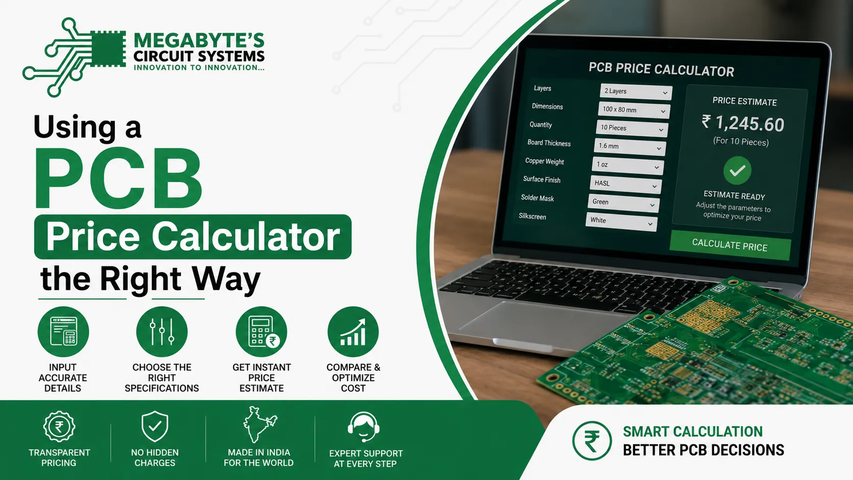
One thing I see quite often is procurement teams entering incorrect data into an online quote tool and getting a shock later. To get an accurate estimate for PCB Manufacturing, you need to know exactly what parameters to feed the system.
Here is what you need ready before you open our PCB Calculator:
Whenever you want to validate a budget, just upload your Gerber files directly into a reliable calculator rather than guessing the specs. It prevents unpleasant surprises during production.
Quick Technical Summary: Accurate PCB cost estimation requires precise inputs of X/Y dimensions, finished copper weight, board thickness, and via types. Utilizing a dedicated PCB calculator with exact Gerber data prevents quote discrepancies and budgeting errors.
As a manufacturer, we want your boards to yield perfectly on the first run. The higher our yield, the lower your price. Here is my personal engineer’s checklist for cost-optimized fabrication in India:
Quick Technical Summary: Cost-effective Design for Manufacturing (DFM) relies on smart panelization, utilizing standard through-hole vias, limiting unique drill sizes, and maintaining generous edge clearances. These practices maximize factory yield and lower the per-unit cost.
I’ve seen startups try to save 10% on their order by skipping electrical testing. Let me tell you straight: a dead board costs you infinitely more in troubleshooting time and replaced components than the small amount you saved on testing.
At Megabyte Circuit Systems, we adhere to strict standards.
Quality manufacturing in India has reached global parity. You no longer need to ship files overseas and deal with customs delays to get a precision-crafted, reliable board.
Quick Technical Summary: Reliable PCB fabrication requires adherence to IPC-A-600 Class 2 standards, 100% Electrical Testing (E-Test) for continuity, and Automated Optical Inspection (AOI). Skipping these quality checks to lower upfront costs often results in expensive post-assembly failures.
The “Make in India” initiative has completely transformed our supply chain. Lead times are shorter, and domestic sourcing of laminates has stabilized.
To get the best pricing from a domestic fabricator:
For standard 2-layer FR-4 boards in medium volume, the cost usually ranges between ₹10 to ₹30 per square inch. This varies widely based on trace constraints, copper weight, surface finish, and whether the order is a small prototype batch or mass production.
Prototyping carries fixed engineering (CAM) and tooling costs that are divided among just a few boards. When you order 1,000 units, those fixed setup costs are spread out, making the variable material cost the primary factor, drastically lowering the per-board price.
If your design includes fine-pitch surface mount components, BGA packages, or requires wire bonding, ENIG provides a perfectly flat surface and prevents oxidation for up to 12 months. For simple through-hole designs, standard HASL is more than sufficient and saves money.
To achieve affordable fabrication, stick to a 2-layer design if possible, use standard 6/6 mil trace and space, limit unique drill hole sizes, and utilize a standard 1.6mm FR-4 thickness. Consolidating your orders to increase volume also significantly drives down unit prices.Yes. While this guide focuses on bare board fabrication, we offer end-to-end solutions. Once your bare boards are fabricated, we can populate them using our automated SMT lines.
Most Indian manufacturers consider 6 mil (0.15mm) trace and spacing as standard capability. Dropping below this to 4 mil or 3 mil requires advanced etching controls and High-Density Interconnect (HDI) processes, which will incur a premium charge.
Pricing a PCB doesn’t have to be a guessing game. When you understand the math behind layer counts, surface finishes, and factory tooling, you can design smarter and budget accurately. Whether you are spinning your very first prototype or pushing for a 10,000-unit production run, having a reliable local partner changes the game.
In my two decades here in Ahmedabad, I’ve seen exactly what happens when engineers get the right manufacturing support—innovations hit the market faster and with fewer headaches.
If you are ready to move forward, skip the guesswork. Head over to our online portal, upload your Gerber files, and let us show you exactly what world-class, Make-in-India manufacturing looks like. We are Megabyte Circuit Systems, and we are ready to build your next breakthrough.
C/10, Yogeshwar Estate, B/H Madhuram Estate, Nr. Vishala Estate, Sardar Patel Ring Rd, Odhav, Ahmedabad, Gujarat, Ahmedabad - 382430, Gujarat (India)
Copyright © 2025. Megabytes Circuit Systems All rights reserved.
Powered by FrogMEE Tech