Ahmedabad - 382430, Gujarat (India)

Hardware is hard. If you are an IoT founder, a hardware engineer, or an R&D procurement manager, you already know this. You also know that when you are in the middle of a development cycle, every single day counts. Waiting weeks for a prototype to clear customs or paying exorbitant fees for standard iterations can absolutely kill your project’s momentum.
In my 20+ years of hands-on experience in PCB fabrication at Megabyte Circuit Systems right here in Ahmedabad, I’ve seen hundreds of brilliant hardware designs delayed simply because the prototyping phase wasn’t optimized. Hardware engineers and students alike often struggle to find a reliable PCB prototyping India partner that balances speed, cost, and industrial-grade quality.
This guide isn’t just theory. I’m going to sit down with you and explain exactly how to optimize your Gerber files, choose the right stack-up, and leverage local manufacturing to get a fast PCB prototyping service without blowing your R&D budget. Let’s get your boards fabricated the right way, the first time.
Quick Technical Summary: Fast PCB prototyping accelerates the hardware iteration cycle, drastically reducing time-to-market. Utilizing a local PCB prototype service in India eliminates international shipping delays and customs bottlenecks, providing engineers with immediate physical validation of their electronic designs.
When you design a new circuit, simulations in SPICE or Altium can only take you so far. Real-world variables like electromagnetic interference (EMI), thermal dissipation, and parasitic capacitance only reveal themselves when you have physical copper and FR4 in your hands.
A pcb prototype service is essentially your safety net. Going straight to mass production without a prototype is a gamble I never recommend to my clients. Even a simple silkscreen error or a swapped footprint can render 5,000 boards useless. Rapid prototyping allows you to:
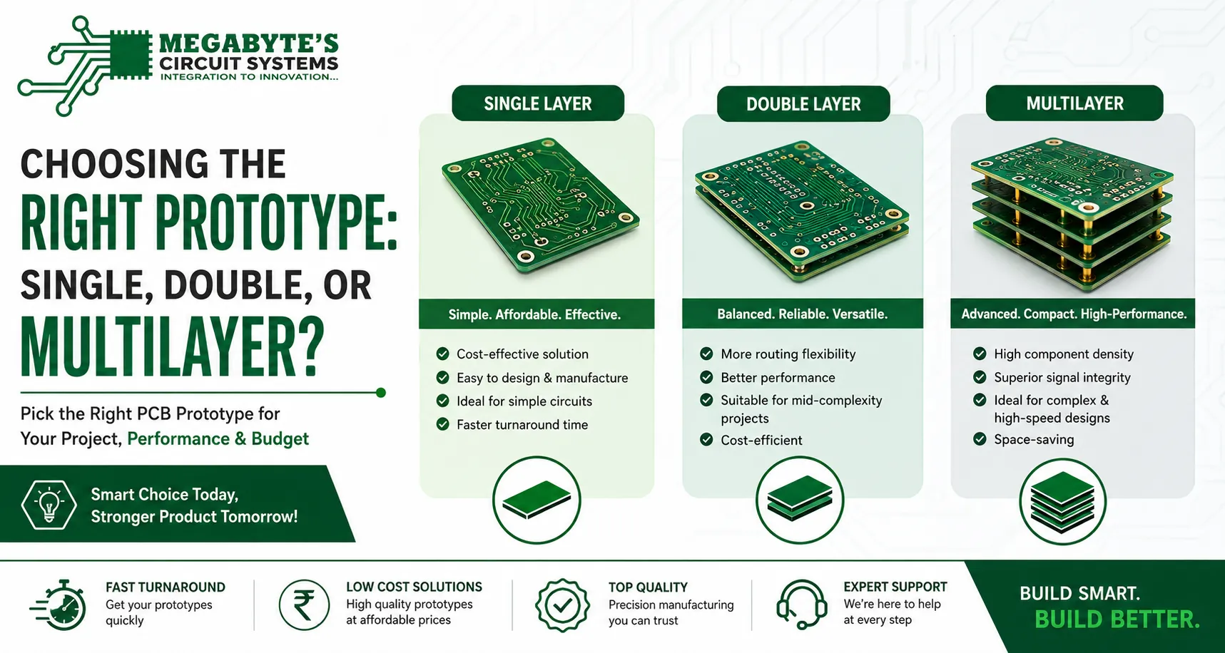
Quick Technical Summary: Selecting the correct layer count for your prototype directly impacts manufacturing complexity, cost, and lead time. Startups must balance signal integrity requirements against fabrication costs when transitioning from simple prototypes to complex multilayer stacks.
One thing I always tell my clients is to not over-engineer the prototype if you don’t have to. The type of board you choose drastically changes the fabrication timeline.
If you are working on a simple power supply or a basic LED driver, a Single Layer PCB is incredibly fast to produce and offers the absolute lowest cost. For standard microcontroller projects and most IoT sensor nodes, a Double Layer PCB with Plated Through Holes (PTH) is the industry standard, offering a perfect balance of routing flexibility and low cost.
However, as you move into high-speed digital designs, FPGAs, or dense BGA packages, you will inevitably need a Multilayer PCB. While multilayer boards take slightly longer to fabricate due to the lamination processes, they are non-negotiable for controlled impedance and proper grounding.
Feature | Single Layer | Double Layer | Multilayer (4-8+ Layers) |
Routing Density | Low | Medium | High to Ultra-High |
Prototyping Cost | Very Low | Low | Moderate to High |
Lead Time | 24 – 48 Hours | 2 – 4 Days | 5 – 10 Days |
Best Used For | Simple analog, basic lighting | IoT nodes, motor drivers, MCU boards | High-speed digital, RF, dense SMDs |
Signal Integrity | Poor (No ground plane) | Good (can pour ground) | Excellent (Dedicated GND/VCC planes) |
Quick Technical Summary: A strict Design for Manufacturing (DFM) checklist prevents costly respins, CAM holds, and fabrication delays. Key optimization areas include standardizing trace widths, maintaining adequate annular rings, and adhering to standard FR4 material specifications.
The secret to a low cost pcb prototype is ensuring your design slides through our CAM (Computer-Aided Manufacturing) department without raising any red flags. When we have to pause production to email you about a drill hit that is too close to a copper pour, you lose time.
Before you export your Gerber RS-274X files, run through this engineer’s checklist:
By adhering to standard Design for Manufacturing principles, you ensure a frictionless transition into our PCB Manufacturing service later on when you are ready to scale to thousands of units.
Quick Technical Summary: Even for rapid, low-cost prototypes, rigorous quality control like Flying Probe Testing (FPT) and E-testing is mandatory. Ensuring prototypes meet IPC-A-600 standards guarantees that the physical board behaves exactly like the digital CAD design.
There is a common misconception that because a board is “just a prototype,” it doesn’t need stringent testing. I strongly disagree. If your prototype has a hidden short or an open circuit due to poor manufacturing, you will waste days debugging your firmware or replacing expensive ICs, completely unaware that the bare board is the actual culprit.
At Megabyte Circuit Systems, every single prototype goes through E-testing. For small batches, we utilize Flying Probe Testing. Unlike a bed-of-nails fixture (which is expensive and reserved for mass production), a flying probe uses robotic arms to physically touch the pads and test for continuity and isolation. We strictly adhere to IPC-A-600 standards, ensuring that your prototype copper adheres properly, the solder mask is cured, and the vias are uniformly plated.
Quick Technical Summary: Engineers can minimize fast prototyping costs by utilizing standard FR4 TG130 materials, sticking to 1oz copper weight, and avoiding blind or buried vias. Utilizing online calculators helps estimate fabrication costs transparently before placing an order.
If you are looking for a highly efficient and low cost pcb prototype, standardization is your best friend. Every time you deviate from standard manufacturing materials, the cost goes up because we have to interrupt our standard panel pooling process.
Here are my top tips for keeping your R&D budget intact:
To get an immediate grasp of your costs, I highly recommend using our PCB Calculator. It allows you to input your exact dimensions, layer count, and specifications to get a transparent estimate instantly.
Quick Technical Summary: Partnering with an experienced, local PCB manufacturer in India ensures rapid communication, faster logistics, and immediate technical support. A local facility bridges the gap between digital hardware design and physical bare-board realization.
For years, Indian companies defaulted to ordering prototypes from overseas. Today, that is no longer necessary. With geopolitical supply chain shifts and the push for ‘Make in India’, local fabrication has caught up in technology and surpassed overseas options in delivery speed.
When you order a prototype PCB locally, you aren’t just buying a piece of FR4; you are buying the ability to pick up the phone and talk directly to the CAM engineer who is tooling your board. You eliminate the 5-7 days lost to international air freight and customs clearance.
For prototyping, we understand you only need a few boards for testing. Our MOQs for prototypes are extremely flexible, often starting from as few as 5 to 10 pieces, depending on the panel utilization.
We require standard Gerber RS-274X or X2 files, along with an NC Drill file. Ensure you include an outline layer so we know the exact mechanical dimensions and routing path of your board.
Standard lead times for double-sided prototypes range from 3 to 5 working days. However, we do offer expedited fast-track options if you are on a critical deadline and need boards turned around in 24 to 48 hours.
Yes. While this guide focuses on bare board fabrication, we offer end-to-end solutions. Once your bare boards are fabricated, we can populate them using our automated SMT lines.
The most common reasons for CAM holds are missing drill files, trace widths that violate our minimum tolerances, or unplated slots not clearly defined on the mechanical layer. Always double-check your DFM rules before exporting.
Navigating the R&D phase is challenging enough without worrying about manufacturing defects or shipping delays. By optimizing your designs for manufacturing and partnering with a trusted local facility, you can drastically reduce your time-to-market.
At Megabyte Circuit Systems in Ahmedabad, Gujarat, we pride ourselves on supporting the Indian hardware ecosystem with reliable, precision-engineered bare boards. Whether you are an engineering student finalizing a final-year project or a seasoned procurement manager sourcing for an industrial IoT deployment, we are here to help.
Stop waiting weeks for overseas shipments. Upload your Gerber files today, request a quote, and let’s get your prototype onto our production floor.
C/10, Yogeshwar Estate, B/H Madhuram Estate, Nr. Vishala Estate, Sardar Patel Ring Rd, Odhav, Ahmedabad, Gujarat, Ahmedabad - 382430, Gujarat (India)
Copyright © 2025. Megabytes Circuit Systems All rights reserved.
Powered by FrogMEE Tech