Ahmedabad - 382430, Gujarat (India)
If you are a hardware engineer or a procurement manager, you’ve likely faced the classic “Golden Triangle” dilemma: you want it fast, you want it cheap, and you want it to actually work. For years, the default move was to look across the border for high-volume manufacturing. But in my 20+ years at Megabyte Circuit Systems, I’ve seen a massive shift.
The question is no longer just about the lowest price per unit; it’s about the Total Cost of Ownership (TCO). When you factor in shipping delays, customs duties, communication gaps, and the nightmare of a “bad batch” arriving three weeks late, a PCB Manufacturing service based right here in India often emerges as the superior financial and technical choice.
In this guide, I’ll break down exactly how an Indian PCB partner helps you balance your budget while meeting stringent IPC quality standards, and why local expertise is your best defense against project delays.
Most engineers look at the price on a quote and think that’s their final cost. It rarely is. When you work with a global supplier, you are often at the mercy of volatile shipping rates and unpredictable customs clearances.
By choosing a reliable PCB company in India, you immediately eliminate several layers of expenditure:
Choosing an Indian PCB manufacturer reduces the Total Cost of Ownership by eliminating import duties, reducing logistics costs by up to 60%, and ensuring technical support in the same time zone. This local proximity allows for faster Design for Manufacturing (DFM) iterations, which prevents costly production re-runs.
In the world of PCB fabrication, “Quality” isn’t a vague feeling it’s a set of measurable standards. If your manufacturer isn’t talking about IPC-A-600 or ISO 9001:2015, you might be headed for trouble.
At Megabyte, we emphasize that quality starts with the raw material. Whether you are ordering a Single Layer PCB or a high-density interconnect board, the dielectric strength and TG (Glass Transition Temperature) of the FR4 must be verified.
Key standards to verify include:
Feature | Typical Low-Cost Overseas | Premium Indian Manufacturer (Megabyte) |
Material Quality | Recycled or B-grade FR4 | Grade-A KB/Isola/Shengyi Laminates |
Testing | Visual Sampling Only | 100% E-Test / Flying Probe |
Trace Precision | $\pm 20\%$ Variance | $\pm 5\%$ Controlled Impedance |
Support | Ticket-based / Bot-led | Direct Senior Consultant Access |
Lead Time | 15-25 Days (with Shipping) | 3-7 Days (Express Prototyping) |
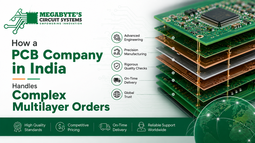
There is a common misconception that India is only good for simple boards. In reality, the technical capability for a Multilayer PCB in India has reached world-class levels.
Managing 4, 6, or 8 layers requires precision in Registration (aligning the layers) and Lamination. If the layers are off by even a few microns, your vias won’t hit the pads correctly. We see this issue very often with startups that try to DIY their first high-speed design.
A professional Indian fab house uses automated optical inspection (AOI) after each layer is etched to ensure no shorts or opens are buried inside the board where you can’t see them. This level of rigor is why many IoT and medical device companies are moving their production back to India.
Modern Indian PCB facilities utilize advanced Lamination Presses and Automated Optical Inspection (AOI) to manufacture high-density Multilayer PCBs with tight tolerances. This ensures structural integrity and signal fidelity for complex high-speed designs while maintaining a localized supply chain.
Time is money, especially during the prototyping phase. If you are waiting three weeks for a prototype, your competitors might already be on their second iteration.
For a specialized PCB Design Service, being in the same time zone means you can have a technical call at 10:00 AM and have a revised design by 2:00 PM. That agility is impossible when dealing with a 12-hour time difference.
I always tell my procurement clients: “Help me help you save money.” Here are three technical ways to lower your quote without touching the quality:
Don’t order individual small boards. Ask your manufacturer to panelize them. This reduces the handling time and material waste. You can even use our PCB Calculator to see how different board dimensions affect the final price.
Unless your design absolutely requires it, try to stay above 6 mil (0.15mm) for trace width and spacing. Moving into the “Ultra-Fine” territory (under 4 mil) requires specialized lithography which increases the scrap rate and, consequently, your price.
For a Double Layer PCB, use the standard 1.6mm thickness with 1oz copper. Deviating to 2.0mm or 2oz copper is sometimes necessary for high-power applications, but it will add a premium to your cost.
Before you hit “Send” on that RFQ, run through this senior consultant’s checklist:
For small to medium batches (prototypes to 5,000 units), India is often cheaper when you include shipping, customs, and the cost of your time. For massive consumer volumes (100k+ units), overseas might have a slight edge on raw unit price, but the risk to your supply chain is significantly higher.
Typically, standard production takes 5–7 working days. However, quick-turn services can deliver prototypes in as little as 24 to 48 hours depending on the complexity and finish (HASL vs. ENIG).
Yes. Modern Indian manufacturers specialize in controlled impedance, high-TG materials, and fine-pitch BGA routing. The key is to provide a detailed stackup requirement during the quoting phase.
You need a complete Gerber folder (Copper layers, Solder Mask, Silk Screen, Drill files, and Board Outline). Providing a “ReadMe” file with your preferred finish (e.g., Lead-free HASL) and copper weight helps speed up the process.
DFM is the bridge between your “ideal” design and a “manufacturable” reality. A good Indian PCB partner will review your files to ensure traces aren’t too close to the board edge and that vias are properly sized, preventing a 0% yield rate.
Choosing the right PCB company in India is about more than just buying a green board; it’s about finding a partner who understands your engineering challenges. At Megabyte Circuit Systems, we pride ourselves on being that partner. From our facility in Ahmedabad, Gujarat, we have spent two decades perfecting the art of high-quality, cost-effective fabrication.
Whether you are looking for a quick-turn prototype or a long-term production partner for your next IoT breakthrough, we are here to help you scale.
C/10, Yogeshwar Estate, B/H Madhuram Estate, Nr. Vishala Estate, Sardar Patel Ring Rd, Odhav, Ahmedabad, Gujarat, Ahmedabad - 382430, Gujarat (India)
Copyright © 2025. Megabytes Circuit Systems All rights reserved.
Powered by FrogMEE Tech