Ahmedabad - 382430, Gujarat (India)
In an era of high-speed processors and 12-layer stackups, it’s easy to overlook the humble 1-layer board. But in my 20+ years at Megabyte Circuit Systems, I’ve seen countless IoT startups and consumer electronics brands over-engineer their products, leading to bloated BOM costs and manufacturing delays.
The truth is, when it’s done right, a Single Layer PCB is often the most elegant solution for cost-sensitive, high-volume production. Whether you are designing a simple LED driver, a power supply, or a basic sensor node, simplicity often translates directly to reliability.
If you are struggling to keep your production costs down or wondering if you can squeeze your design into a single copper layer without signal integrity issues, you are in the right place. I’ll walk you through how we approach 1-layer fabrication here in India and how you can optimize your Gerber files to ensure a 100% yield at our factory.
The most common question hardware engineers ask me during our PCB developing services consultations is: “Can I get away with a single layer?”
The answer depends on your component density and routing complexity. A Single Layer PCB has conductive copper on only one side of the substrate. This means no Vias (Vertical Interconnect Access) are used to jump signals between layers. Every trace must find its path without crossing another.
If your design involves:
…then a single layer is your best friend. However, if you have a dense BGA or high-speed differential pairs, you likely need a Double Layer PCB to provide a dedicated ground plane for EMI shielding.
Single Layer PCBs utilize a single conductive copper layer on one side of a dielectric substrate (usually FR4 or MCPCB). They are the most cost-effective solution for low-density designs, offering higher reliability in thermal dissipation and easier troubleshooting compared to multi-layer alternatives.
You’d be surprised how much of the world still runs on 1-layer technology. In the Indian market, where price-to-performance ratio is king, we see these boards used everywhere:
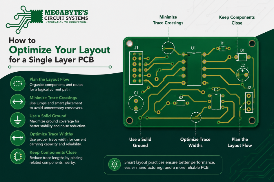
One thing I always tell my clients is that a single-layer layout is actually harder to design than a multi-layer one. Why? Because you can’t “cheat” by using vias to solve routing dead-ends.
In a 1-layer design, zero-ohm resistors or wire jumpers are your only way to “cross” traces. Use them sparingly, but strategically. Place them in areas where they won’t interfere with automated pick-and-place machines if you are opting for a full PCB Assembly service.
For single-layer boards, we often use thicker laminates. To prevent etching issues, I recommend a minimum trace width and spacing of 8 mil (0.2mm). While we can go lower at Megabyte, staying at 8 mil or higher significantly improves your manufacturing yield and reduces costs.
Even without a dedicated ground layer, you should use a copper pour on your signal layer. This helps with EMI and reduces the amount of etchant chemical we need to use, which is better for the environment and the board’s structural integrity.
Feature | Single Layer | Double Layer | Multilayer (4+) |
Manufacturing Cost | Lowest | Moderate | High |
Design Complexity | High (Routing logic) | Low to Moderate | High (Signal Integrity) |
Lead Time | Fastest (24-48 hours) | Standard | Longer |
Ideal Use Case | Power/LED/Simple IoT | General Electronics | High-Speed Computing |
EMI Shielding | Poor | Good | Excellent |
Single Layer PCBs offer the fastest manufacturing turnaround and the lowest unit cost, but require more creative routing due to the absence of signal layers. While they lack the built-in EMI shielding of a Multilayer PCB, they are superior for high-current and thermal-intensive applications.
Before you upload your files to our PCB Calculator, check these three things:
Being a premier PCB Manufacturing service in Ahmedabad, we understand the Indian electronics ecosystem. Here is how you can drive your costs down even further:
Absolutely. In fact, many modern LED drivers are 100% SMD on a single layer. Just remember that your components and traces will all be on the same side, so plan your routing carefully to avoid “trapped” pads.
No. While FR4 is the most common, we also use Paper Phenolic (FR1/FR2) for extremely low-cost toys and Metal Core (Aluminum) for high-power LED applications where heat management is critical.
By definition, a single layer board doesn’t need to connect one layer to another, so the holes are usually NPTH (Non-Plated Through Holes). This actually makes the board cheaper to produce as it skips the electroless copper plating step.
We see this issue very often where a client needs a board “yesterday.” For standard single-layer designs, we can often ship within 24 to 48 hours from our Ahmedabad facility.
If your design isn’t too dense, it’s worth a try! If you’re stuck, our team can help review your schematic to see if a single-layer conversion is feasible to save production costs.
Simplicity shouldn’t mean a sacrifice in quality. Whether you are building a simple prototype or scaling to 10,000 units, a Single Layer PCB from Megabyte Circuit Systems ensures you get the best of Indian manufacturing: speed, precision, and unbeatable value.
We’ve helped hundreds of engineers across India from the hardware hubs of Bangalore to the industrial belts of Gujarat bring their products to life.
Ready to see the difference experience makes?
Let’s get your project moving!
C/10, Yogeshwar Estate, B/H Madhuram Estate, Nr. Vishala Estate, Sardar Patel Ring Rd, Odhav, Ahmedabad, Gujarat, Ahmedabad - 382430, Gujarat (India)
Copyright © 2025. Megabytes Circuit Systems All rights reserved.
Powered by FrogMEE Tech