Ahmedabad - 382430, Gujarat (India)
If you are a hardware engineer running a high-speed digital design simulation, an IoT startup founder pitching a smart-metering solution, or a procurement manager tracking a critical industrial supply chain, you have likely noticed a massive shift. The old hardware playbook designing a circuit board in India and automatically outsourcing fabrication to overseas hubs is rapidly changing.
The pressure on engineering teams today is intense. You are dealing with tighter component lead times, complex Design for Manufacturing (DFM) constraints, and an urgent requirement to meet international quality standards like IPC Class 2 or Class 3. Historically, sourcing high-reliability boards domestically meant balancing a painful trade-off between local speed and global quality.
Over my 20+ years in PCB fabrication, I have sat down with hundreds of Indian engineers who faced this exact bottleneck. They would tell me, “We want to build in India, but our high-density interconnect (HDI) boards or controlled-impedance multilayer stacks need to meet rigorous global standards without dropping the ball on yield rates.”
Today, top-tier pcb manufacturers in india have systematically closed that gap. By upgrading to automated optical inspection (AOI), investing in advanced direct imaging (DI) systems, and implementing strict international quality protocols, domestic fabrication facilities are successfully scaling up to handle complex global demands. Let’s break down exactly how Indian manufacturing has evolved, what technical standards govern high-yield production today, and how you can optimize your designs to get the best out of modern Indian fabrication facilities.
For a long time, the domestic manufacturing ecosystem was primarily associated with quick-turn prototyping or simpler single- and double-sided boards. If an industrial application required a high-density 8-layer board with 4-mil trace widths and laser-drilled microvias, the default assumption was to source it internationally.
Today, that narrative has shifted completely. Modern production facilities are operating at a completely different tier of precision. The integration of advanced computer-aided manufacturing (CAM) software, automated chemical plating lines, and climate-controlled cleanrooms (Class 10,000 or better) allows domestic teams to scale from low-volume engineering builds straight into high-volume, global-ready mass production.
This maturation of the local supply chain means you no longer have to navigate the hidden friction points of cross-border sourcing such as unexpected customs delays, volatile shipping costs, or frustrating communication gaps across time zones. Instead, you can collaborate directly with a local technical partner who reviews your Gerber files, identifies potential assembly bottlenecks before the physical panels hit the plating tanks, and keeps your project moving smoothly on the factory floor.
Quick Technical Summary
Leading Indian PCB fabricators have scaled their operations by upgrading to direct imaging (DI) technology and automated optical inspection (AOI) lines. These advancements enable the domestic production of complex, high-reliability boards featuring tight trace tolerances and controlled impedance. Consequently, engineering teams can seamlessly transition from quick-turn prototyping to high-volume manufacturing within a single unified domestic ecosystem.
When we talk about global standards in electronics manufacturing, we are primarily talking about the IPC framework. IPC standards govern everything from design guidelines to target criteria for surface acceptability. If your boards cannot reliably pass these metrics, your product cannot compete effectively in international markets.
For the vast majority of industrial, commercial, and IoT applications, IPC-A-600 Class 2 is the benchmark standard. It dictates acceptable dimensional tolerances, dielectric thicknesses, and component pad conditions. However, if you are designing for critical automotive sub-systems, aerospace, or medical electronics, your designs must meet the stringent requirements of IPC Class 3.
Achieving Class 3 compliance requires absolute control over every stage of the fabrication process:
IPC Class 2 (Standard Industrial) –> Allows minimal annular ring breakout
IPC Class 3 (High Reliability) –> Zero breakout permitted + 1-mil minimum copper plating in PTH
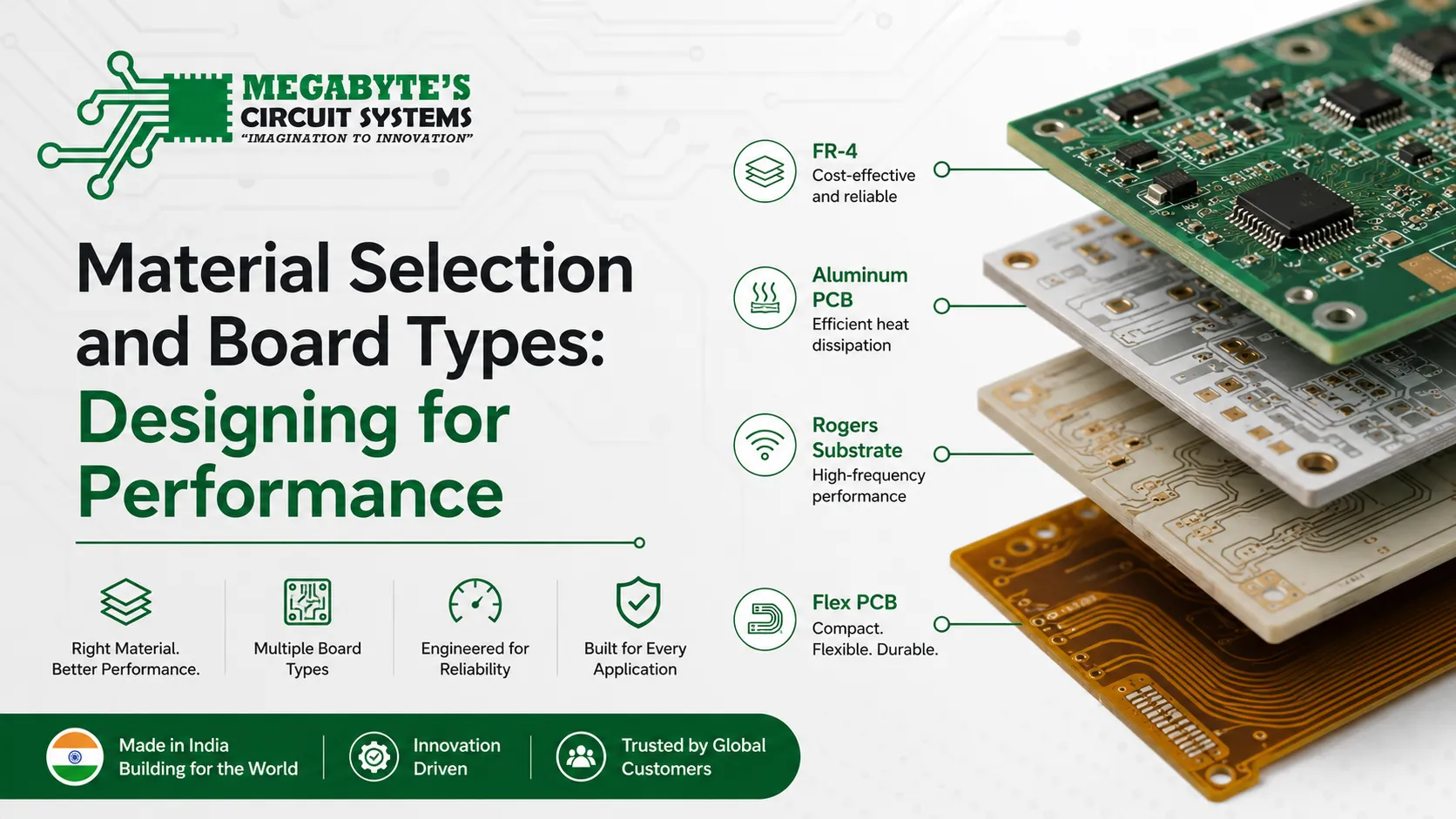
A major factor in scaling production to global standards is selecting the right material stack-up for your specific application. The choice of substrate affects everything from thermal dissipation to signal integrity at high frequencies.
Whether your system requires a cost-effective Single Layer PCB for a straightforward consumer product, a durable Double Layer PCB for an industrial controller, or a highly dense Multilayer PCB for a high-speed computing application, selecting the appropriate material and layer structure early in the design cycle is vital for maximizing manufacturing yields.
Attribute | Single Layer PCB | Double Layer PCB | Multilayer PCB (4 to 12+ Layers) |
Typical Material | Standard FR-4, CEM-1, Aluminum | FR-4, High-Tg FR-4 | High-Tg FR-4, Rogers, PTFE |
Minimum Trace / Space | 6 mil / 6 mil | 4 mil / 4 mil | 3 mil / 3 mil (Advanced) |
Via Capabilities | None (Non-PTH holes only) | Standard PTH, Blind Vias | PTH, Blind Vias, Buried Vias, Microvias |
Impedance Control | Rarely Required | Optional ($\pm 10\%$) | Strictly Managed ($\pm 5\%$ to $\pm 10\%$) |
Primary Applications | Power supplies, simple LED drivers | Industrial automation, IoT nodes | High-speed computing, telecommunications |
Choosing the correct substrate whether High-Tg FR-4 for thermal stability, aluminum-core for high-power dissipation, or low-loss PTFE for RF applications directly dictates the reliability of your board. Selecting the right board type and matching it to production tolerances early ensures your design remains robust during automated assembly and field operations.
One thing I always tell my clients is that a beautiful design on a high-end CAD screen doesn’t automatically translate to a high-yield run on the factory floor. The true secret to scaling electronic manufacturing to global standards lies in strict adherence to Design for Manufacturing (DFM) principles.
When you send your Gerber or ODB++ files to a professional PCB Manufacturing service, a dedicated front-end engineering team processes your files through CAM software to flag DFM violations. Catching these issues before production begins saves valuable time and prevents costly material waste.
A PCB manufacturer cannot claim global status without implementing robust, non-destructive testing and verification pipelines on 100% of the production panels. Visual inspection alone is completely inadequate for modern high-density designs.
Top-tier domestic operations rely on a multi-stage quality assurance process:
Achieving global reliability requires modern PCB fabricators to deploy automated optical inspection (AOI) alongside 100% electrical testing (E-test via flying probe or hard fixtures). These non-destructive testing steps ensure that internal layer registration, trace continuity, and insulation resistances match the design files exactly before shipment.
Managing your project costs while scaling up quality is a delicate balancing act. Many engineering teams inadvertently drive up their fabrication expenses by over-specifying tolerances that their application doesn’t actually require. To optimize your hardware budget, consider these highly practical steps:
For standard 4 to 8 layer prototypes, quick-turn fabrication services can routinely deliver finished boards within 3 to 5 working days. Mass production lead times generally range between 2 to 3 weeks, depending entirely on material availability, layer complexity, and the selected surface finish.
When signal switching speeds rise or frequencies enter the RF domain, PCB traces act as transmission lines rather than simple wires. Controlled impedance testing ensures that the physical trace width, dielectric height, and copper thickness match your target impedance (e.g., $50\Omega$ single-ended or $100\Omega$ differential pair) within a tight tolerance, preventing signal reflections and data corruption.
ENIG is highly recommended for designs featuring fine-pitch surface mount components, Ball Grid Arrays (BGAs), or small 0201/01005 passives because it provides an exceptionally flat, coplanar surface finish. While lead-free HASL is highly robust and cost-effective, its surface can be slightly uneven, which occasionally causes assembly alignment issues on high-density components.
Fabrication facilities utilize pinless lamination systems, specialized x-ray registration verification, and automated optical alignment tools. These systems dynamically adjust the internal film positioning and drill parameters to compensate for the micro-scaling and material shrinkage that naturally occurs when bonding multiple FR-4 core sheets under high pressure and temperature.
While traditional Gerber formats (RS-274X) remain highly reliable and widely accepted across the industry, modern ODB++ or IPC-2581 datasets are generally preferred for complex multilayer boards. These newer formats consolidate layout info, layer stack-up definitions, drill data, and the bill of materials (BOM) into a single, unified database, significantly reducing file translation errors during CAM processing.
Scaling an electronics product to a global standard requires a manufacturing partner who genuinely understands your engineering challenges. At Megabyte Circuit Systems, based in our state-of-the-art facility in Ahmedabad, Gujarat, we have spent decades refining our processes to bridge the gap between complex hardware design and flawless physical production.
Whether you need a specialized PCB Design Service to optimize a high-speed layout, advanced PCB Developing Services to refine your early-stage concepts, or a complete, end-to-end PCB Assembly service to deliver fully populated, tested assemblies directly to your production line, our team is equipped to support your journey. We don’t just print circuits; we work closely alongside your engineering team to ensure your designs achieve maximum yield, complete IPC compliance, and seamless scalability.
Ready to take your next hardware project from the layout screen to volume manufacturing? Let’s collaborate. Reach out to our engineering team today to discuss your technical specifications, use our instant online tools, or upload your Gerber files to receive a comprehensive, DFM-vetted manufacturing quote.
C/10, Yogeshwar Estate, B/H Madhuram Estate, Nr. Vishala Estate, Sardar Patel Ring Rd, Odhav, Ahmedabad, Gujarat, Ahmedabad - 382430, Gujarat (India)
Copyright © 2025. Megabytes Circuit Systems All rights reserved.
Powered by FrogMEE Tech