Ahmedabad - 382430, Gujarat (India)
If you are building an IoT device, a smart EV charger, or a custom industrial automation module, you already know that moving from a breadboard prototype to a mass-market product is a minefield. You design your schematics, run simulations, and carefully layout your traces. But when it comes to actual fabrication, a critical question pops up: Should we import cheap boards, or should we partner with a local manufacturer?
In my 20+ years of managing PCB fabrication at Megabyte Circuit Systems, I’ve sat down with hundreds of Indian hardware founders and electronics engineers. I’ve seen bright startups lose momentum not because their circuit design was flawed, but because their imported boards arrived with misaligned vias, delayed shipping, or sudden customs clearance issues.
Choosing a local PCB Manufacturing service right here in Gujarat isn’t just about regional pride. It is a calculated, strategic move that drastically cuts your time-to-market, secures your intellectual property, and keeps your cash flow lean. Let’s break down exactly why partnering with a homegrown manufacturer gives your startup a massive competitive edge.
For an early-stage electronics startup, speed is everything. If your hardware development cycle requires four or five revisions to get the form factor and signal integrity perfectly right, waiting 14 days for an overseas shipment kills your momentum.
When you work with a trusted PCB Manufacturer Gujarat, that 2-week lag drops down to just a few days. Local quick-turn prototyping means you can upload your Gerber files on a Monday and have physical boards on your test bench by Thursday.
We see this issue very often with IoT startups: they find a minor layout error or a component footprint mismatch after the first batch arrives. If you are importing, that mistake costs you another two weeks and thousands of rupees in air freight. Locally, you just tweak the design rules, hop on a phone call with us, and spin a corrected batch immediately.
Local PCB manufacturing in Gujarat accelerates hardware development by slashing prototype turnaround times from weeks to days. This proximity eliminates international shipping friction, allows rapid design iterations, and keeps product launches on schedule.
One thing I always tell my clients is this: What looks flawless on an Altium or Eagle screen doesn’t always translate perfectly to the factory floor. This gap is where Design for Manufacturing (DFM) comes into play.
When you send files to a massive overseas automated portal, no senior engineer reviews your design. If your clearance is too tight or your thermal reliefs are missing, the automated machines print them exactly as drawn resulting in bridges, shorts, or tombstoning components during assembly.
By collaborating with a domestic engineering team, you get real-time DFM support. We review your annular rings, solder mask clearances, and trace widths before the laser photoplotter exposes the panels.
Startups frequently struggle with choosing the right board stackup and material substrate. Over-specifying drives your costs through the roof, while under-specifying leads to cross-talk and signal degradation.
Depending on your product’s architecture, you need to match your design parameters to the right class of board:
PCB Type | Common Applications | Key DFM Considerations | Recommended Material |
LED lighting, basic power supplies, toys | Maximizing trace widths, keeping component spacing generous. | FR4 (Flame Retardant 4) or Aluminum base | |
Industrial controllers, power distribution, IoT gateways | Proper via stitching, solid ground return paths under signal lines. | Standard FR4 (1.6mm thickness, 1oz/2oz copper) | |
Smartphones, high-speed computing, EV battery management | Controlled impedance ($Z_0$), precise dielectric thickness, blind/buried vias. | High-Tg FR4, Isola, or Rogers (for RF designs) |
If you are developing a compact wearable device, a standard two-layer board might cause massive cross-talk due to dense trace routing. Our team can assist you through our specialized PCB Design Service to optimize your stackup, transitioning your layout smoothly into a 4, 6, or 8-layer design that passes all EMI/EMC compliance tests.
Quick Technical Summary
Aligning your hardware architecture with the proper material substrate (FR4 vs. High-Tg) and layer count prevents signal integrity failures. Gujarat-based manufacturers offer direct consultation to help startups balance mechanical constraints with performance requirements.
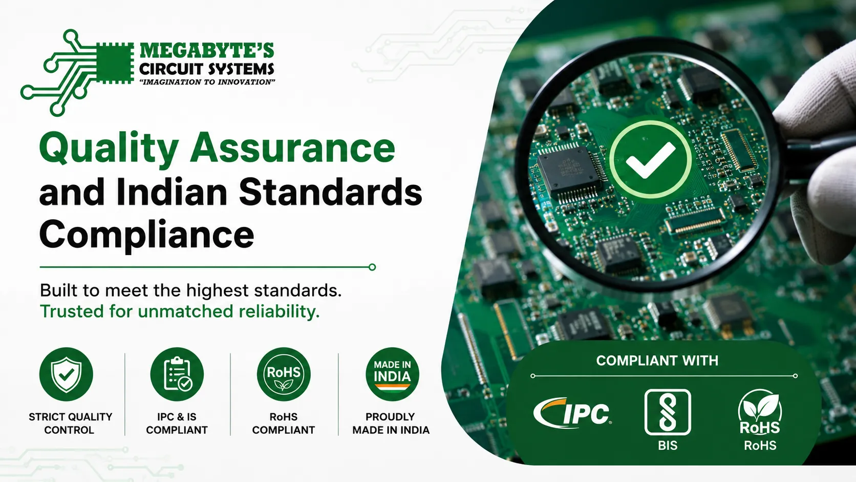
As your startup grows, you will eventually pitch to tier-1 industrial clients or apply for global certifications like CE, UL, or BIS. These bodies don’t just look at your software; they audit your hardware manufacturing trail.
By choosing an established factory in Gujarat, you ensure your boards strictly comply with international and domestic quality standards:
Many hardware founders evaluate overseas prices on a screen without calculating the “landed cost.” When you factor in international air freight, basic customs duties (BCD), social welfare surcharge, integrated GST (IGST), and the inevitable customs clearance delays at ports of entry, the “cheap” option quickly turns expensive.
Landed Cost = Board Unit Cost + Freight + Customs Duties + Clearance Fees + Cost of Delay Time
By establishing a regional supply chain partner in Gujarat:
Partnering with a domestic PCB fabricator eliminates hidden import fees, customs delays, and unpredictable logistics costs. Startups achieve a highly predictable landed cost per board while maintaining lean inventory management.
To get the absolute best lead time and pricing from our manufacturing facility, I always suggest going through this brief technical checklist with your layout engineer before exporting your manufacturing files:
Before you commit to a full panel layout, you can quickly run your parameters through our easy, interactive online PCB Calculator tool to estimate your fabrication costs instantly.
Local manufacturing eliminates long shipping times, unpredictable customs duties, and communication gaps. It provides direct access to expert DFM counseling, allowing you to iterate faster, safeguard your design data, and bring your hardware to market significantly ahead of competitors.
For standard single and double-sided boards, quick-turn prototype fabrication can be completed in as little as 24 to 48 hours. Multilayer designs containing 4 to 8 layers typically require 3 to 5 working days depending on the structural complexity and specific surface finish requested.
Yes. We support hardware startups throughout their entire lifecycle. We offer low-volume prototyping with zero strict MOQs to help you test your designs, and we possess the scalability to handle high-volume commercial production runs smoothly as your business scales up.
If you are using through-hole or larger SMD components and have a tight budget, standard HASL is usually ideal. If your design utilizes fine-pitch surface mount devices, BGAs, or requires a long shelf life before component placement, we strongly recommend ENIG (Gold) surface finishing.
Absolutely. Through our dedicated PCB Developing Services, our design engineers can analyze your schematics, fix trace bottlenecks, optimize ground planes, and modify your design to match native production line limits flawlessly.
Building breakthrough hardware is hard work but managing your supply chain shouldn’t be. At Megabyte Circuit Systems, based in Ahmedabad, Gujarat, we have spent decades turning complex blueprints into highly reliable, high-performance circuit boards. Whether you require a ruggedized single-sided board for power applications or an advanced multi-layered stackup for high-speed computation, our facility is equipped to deliver world-class precision right to your doorstep.
Don’t let your innovative designs get stuck in international transit or delayed by automated fabrication portals. Partner with an expert consulting team that understands your engineering constraints, your timeline, and your business goals.
Ready to launch your next production batch? Upload your Gerber files today, get an instant estimate using our online PCB Calculator, or reach out directly to our engineering office to receive a comprehensive, tailored technical quote.
C/10, Yogeshwar Estate, B/H Madhuram Estate, Nr. Vishala Estate, Sardar Patel Ring Rd, Odhav, Ahmedabad, Gujarat, Ahmedabad - 382430, Gujarat (India)
Copyright © 2025. Megabytes Circuit Systems All rights reserved.
Powered by FrogMEE Tech