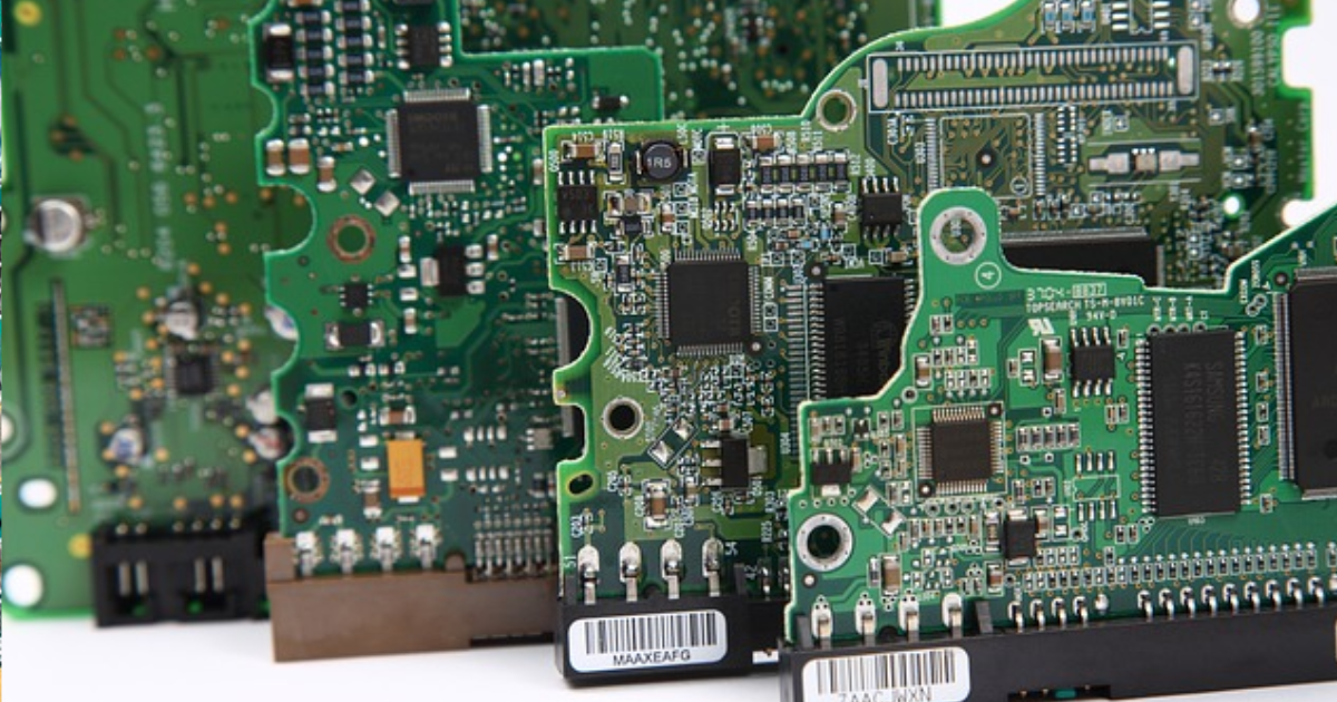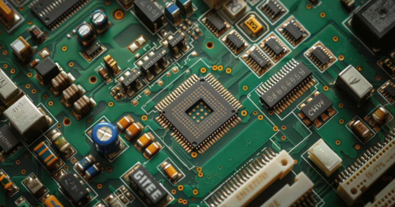
Prototype PCB in India: How to Get Started with Your First Board
For startups, hobbyists, and engineers, creating a prototype PCB in India is a critical step in turning innovative ideas into functional products. A prototype printed circuit board (PCB) is a preliminary version of a circuit board used to test designs before mass production. With India emerging as a hub for electronics manufacturing, prototyping has become more accessible and cost-effective. Whether you’re designing a smart device, IoT module, or medical equipment, understanding the prototyping process in India can save time, reduce costs, and ensure quality.
This comprehensive guide walks you through the process of creating your first prototype PCB in India, covering local manufacturers, costs, challenges, and a step-by-step approach. By leveraging India’s growing PCB industry, you can bring your vision to life efficiently. Ready to start your prototyping journey? Contact us for expert PCB fabrication services.
Why Choose India for PCB Prototyping?
India’s electronics sector is booming, driven by government initiatives like “Make in India” and a skilled workforce. Here’s why PCB board fabrication in India is ideal for prototyping:
- Cost-Effectiveness: Lower labor and material costs make India a budget-friendly option compared to Western markets.
- Local Expertise: Cities like Bangalore, Delhi, and Pune host numerous PCB manufacturers with advanced facilities.
- Quick Turnaround: Proximity to local suppliers ensures faster delivery, often within days for prototypes.
- Growing Infrastructure: Investments in automation and technology have improved the quality of PCB fabrication in India.
For startups and hobbyists, these advantages make India an attractive destination for prototyping innovative electronics.
Step-by-Step Guide to Creating Your First Prototype PCB in India
Follow this detailed process to develop your first prototype PCB in India, from concept to finished board.
Step 1: Define Your PCB Requirements
Before contacting a manufacturer, clarify your project’s specifications:
- Board Type: Single-layer, double-sided, or multilayer PCB.
- Size and Shape: Determine dimensions and any custom shapes.
- Components: List components (e.g., resistors, ICs) and their placement needs.
- Performance Needs: Specify signal speed, power requirements, or thermal constraints.
- Quantity: Decide how many prototype boards you need (typically 1–10 for initial testing).
Tip: Use a checklist to ensure all requirements are documented. This helps manufacturers provide accurate quotes.
Step 2: Design Your PCB
Use PCB design software to create your schematic and layout:
- Popular Tools: KiCad (free), Altium Designer, or Eagle for professional designs.
- Key Design Considerations:
- Ensure proper trace widths for current capacity.
- Optimize via placement to avoid signal interference.
- Include test points for debugging.
- Design Rule Check (DRC): Run DRC to catch errors like overlapping traces or incorrect spacing.
Case Study: A Bangalore-based startup designing an IoT sensor used KiCad to create a 4-layer prototype PCB, reducing design costs by 30% compared to proprietary software.
Step 3: Select a Reliable PCB Manufacturer in India
Choosing the right manufacturer is critical for quality and reliability. Look for:
- Experience: Manufacturers with a track record in prototype PCB in India.
- Capabilities: Support for multilayer boards, surface-mount technology (SMT), and quick-turn services.
- Certifications: ISO 9001 or IPC standards for quality assurance.
- Customer Reviews: Check testimonials or case studies for credibility.
Top Indian Manufacturers:
- PCB Power Market (Ahmedabad): Known for quick-turn prototypes and online ordering.
- CEM Solutions (Bangalore): Specializes in multilayer PCBs for startups.
- Sion Semiconductors (Hyderabad): Offers end-to-end prototyping and assembly.
Tip: Request quotes from multiple manufacturers to compare pricing and lead times. Get a quote from our trusted PCB fabrication services.
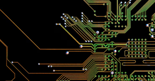
Step 4: Generate and Submit Gerber Files
Gerber files are the industry-standard format for PCB manufacturing. They include:
- Copper layers
- Solder mask
- Silkscreen
- Drill files
Use your design software to export Gerber files and verify them using a Gerber viewer (e.g., Gerbv). Submit these files to your chosen manufacturer along with a Bill of Materials (BOM) listing all components.
Common Mistake: Incomplete Gerber files can delay production. Double-check that all layers are included.
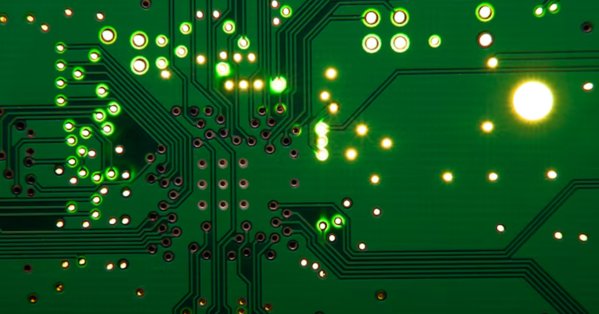
Step 5: Prototype Fabrication
The manufacturer will fabricate your PCB based on the provided files. The process includes:
- Material Selection: FR-4 is common for prototypes due to its affordability and durability.
- Fabrication: Etching copper layers, drilling vias, and applying solder mask.
- Quality Checks: Automated optical inspection (AOI) to detect defects.
Lead times for PCB board fabrication in India typically range from 3–10 days for prototypes, depending on complexity.
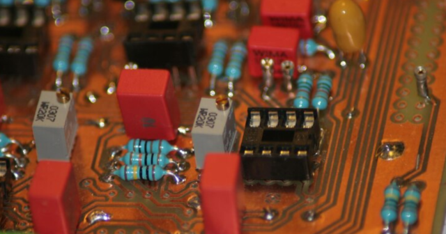
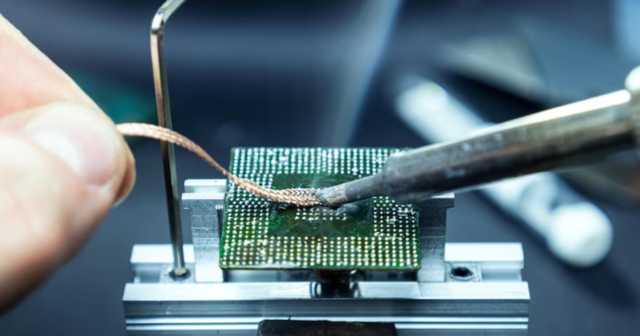
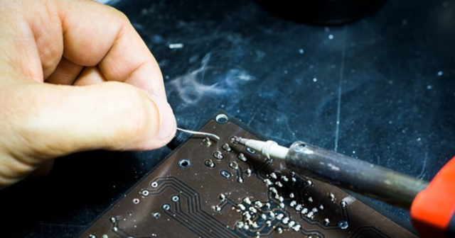
Step 6: Assembly and Component Sourcing
After fabrication, components are mounted on the board:
- Manual Assembly: Suitable for small batches or complex designs.
- SMT Assembly: Automated for high precision and speed.
- Component Sourcing: Manufacturers may source components, or you can provide them. Local distributors like Element14 India offer quick access to parts.
Testimonial: “We partnered with a Delhi-based PCB fabricator for our prototype. Their SMT assembly saved us 40% on production time,” says Anil K., a startup founder.
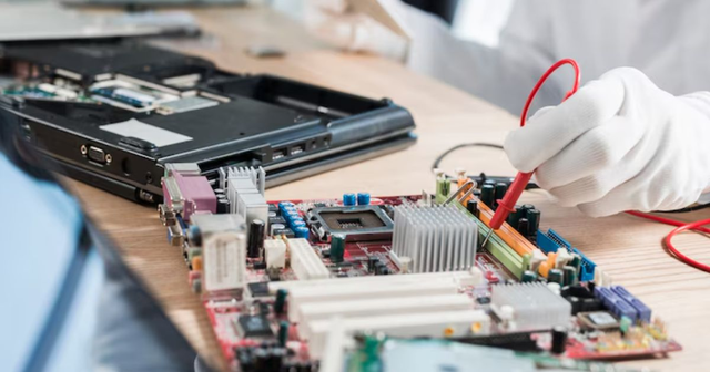
Step 7: Testing and Validation
Test your prototype to ensure it meets design expectations:
- Functional Testing: Verify circuit performance using multimeters or oscilloscopes.
- Environmental Testing: Check for thermal or vibration resistance if needed.
- Debugging: Identify and fix issues like short circuits or signal noise.
Tip: Order extra prototype boards to test multiple iterations and avoid delays.
Step 8: Iterate and Scale
Based on test results, refine your design and order additional prototypes if needed. Once satisfied, transition to small-batch or full-scale production with the same manufacturer to maintain consistency.
Costs of Prototype PCB in India
The cost of prototype PCB in India depends on several factors:
- Board Complexity: Single-layer boards cost $10–$50, while multilayer boards range from $50–$200 for prototypes.
- Quantity: Small batches (1–5 boards) are pricier per unit than larger orders.
- Turnaround Time: Express services (24–48 hours) increase costs by 20–50%.
- Assembly: SMT assembly adds $20–$100, depending on component count.
Example: A 2-layer, 10×10 cm prototype with SMT assembly typically costs $30–$80 in India, compared to $100–$200 in the US.
Tip: Use a PCB cost calculator to estimate expenses and optimize your design for cost savings. Try our PCB cost calculator today.
Challenges in PCB Prototyping in India
While India offers many advantages, prototyping can face challenges:
- Quality Variability: Some low-cost manufacturers may compromise on quality. Solution: Choose certified vendors with positive reviews.
- Supply Chain Delays: Component shortages can delay assembly. Solution: Partner with manufacturers who offer in-house sourcing.
- Design Errors: Incorrect Gerber files or poor design can lead to faulty boards. Solution: Use DRC and consult with manufacturers during the design phase.
- Communication Gaps: Misunderstandings with manufacturers can cause delays. Solution: Provide clear specifications and maintain regular contact.
Case Study: A Pune-based hobbyist faced delays due to incomplete Gerber files. By working closely with their manufacturer’s design team, they resolved the issue and received their prototype in 5 days.
Tips for Successful PCB Prototyping in India
- Start Small: Begin with a simple design to test the prototyping process.
- Leverage Local Expertise: Collaborate with manufacturers for design feedback.
- Plan for Iterations: Budget for multiple prototype rounds to perfect your design.
- Explore Online Platforms: Websites like PCB Power Market allow easy ordering and tracking.
- Stay Updated: Follow industry trends, such as eco-friendly PCBs or automation, to stay competitive.
Why Choose Us for Your Prototype PCB Needs?
At [Your Company Name], we specialize in PCB board fabrication in India, offering quick-turn prototypes tailored to startups and hobbyists. Our ISO-certified facilities and experienced team ensure high-quality boards at competitive prices. Whether you need a single-layer prototype or a complex multilayer design, we’re here to help. Request a quote for your prototype PCB today.
Conclusion
Creating a prototype PCB in India is an exciting opportunity for startups and hobbyists to innovate affordably. By following the step-by-step process defining requirements, designing, selecting a manufacturer, and testing you can develop a high-quality prototype that sets the stage for successful production. India’s cost-effective manufacturing, skilled workforce, and growing infrastructure make it an ideal destination for PCB prototyping.
Overcome challenges like quality variability and supply chain delays by partnering with reputable manufacturers and leveraging tools like PCB design software and cost calculators. Ready to bring your idea to life? Contact us for expert PCB prototyping services and start building your future today.