Ahmedabad - 382430, Gujarat (India)
If you have ever had an assembly line halt because a batch of boards was delayed at customs, or if you have opened a shipment only to find warped substrates and delaminated traces, you know that electronics manufacturing isn’t just an engineering challenge it is a logistical high-wire act.
When managing hardware pipelines for hardware engineers, IoT startups, and industrial procurement managers across India, the bridge between a perfect Gerber file and a scalable, production-ready product is entirely dependent on your supply chain. In my 20+ years of hands-on experience in electronics manufacturing, I have sat down with hundreds of engineering teams.
The truth is, a brilliant schematic means nothing if your manufacturing partner cannot consistently source copper clad laminates, manage multi-layer stackups, handle quick-turn prototyping, and deliver on time without surprise costs.
This comprehensive guide breaks down the complex mechanics of pcb board manufacturing india, from raw material procurement to final factory delivery. Whether you are scaling an industrial IoT gateway or optimizing a commercial lighting product, this framework will help you de-risk your hardware pipeline, cut lead times, and optimize your procurement spend.
The foundation of any high-reliability circuit board is its raw material substrate. In India, the component ecosystem relies heavily on predictable material sourcing. When selecting laminates, engineering teams often default to standard specifications without considering environmental conditions, such as the high humidity and ambient temperatures typical of industrial environments across India.
Choosing the right grade of FR-4 (Flame Retardant 4) is critical. For standard consumer electronics or commercial lighting, standard FR-4 with a Glass Transition Temperature ($T_g$) of 130°C to 140°C is perfectly adequate. However, if you are designing industrial automotive modules, solar inverters, or telecommunication hardware, you must specify High-$T_g$ FR-4 ($T_g > 170^\circ\text{C}$) to prevent thermal expansion from tearing apart your plated-through holes (PTH) or damaging delicate surface-mount device (SMD) joints.
Beyond base FR-4, specialized high-frequency or high-power applications require alternative substrates. For high-power RF or microwave circuits, standard glass-weave substrates exhibit unacceptably high dielectric loss, making specialized PTFE-based materials necessary. For high-output LED drivers or power converters, an aluminum-core insulated metal substrate (IMS) is essential to pull heat away from active components and maintain system stability.
Quick Technical Summary: Sourcing the correct substrate dictates the thermal and mechanical boundaries of your hardware. High-$T_g$ FR-4 substrates (greater than 170°C) prevent trace delamination and barrel cracks in high-vibration or high-temperature industrial environments.
To help your procurement team select the right substrate before utilizing our PCB Calculator, use this technical matrix to balance performance requirements against cost structures:
Material Type | Common Applications | Key Technical Properties | Supply Chain & Cost Considerations |
Standard FR-4 | Consumer devices, IoT sensors, toys | $T_g$: 135°C–140°C, Dielectric Constant ($D_k$): 4.5 | Readily available in India; lowest cost baseline. |
High-$T_g$ FR-4 | Automotive ECUs, solar inverters, industrial automation | $T_g > 170^\circ\text{C}$, lower thermal expansion ($Z$-axis CTE) | Moderate cost premium; essential for lead-free reflow. |
Aluminum Base (IMS) | LED lighting, power supplies, motor drives | Thermal conductivity: 1.0–3.0 W/m-K | Specialized single-layer processing; prevents thermal runaway. |
High-Frequency (PTFE/Rogers) | RF antennas, radar systems, 5G networking | Low dissipation factor ($D_f \approx 0.002$), stable $D_k$ | Longest sourcing lead times; high cost premium. |
We see this issue very often with growing startups: an engineering team designs an exceptional high-layer-count prototype using an exotic material substrate they found online, only to realize during production optimization that the lead time for that specific material runs into several weeks in the domestic market. Whenever possible, align your designs with robust, locally stocked FR-4 and standard copper weights ($1\,\text{oz}$ or $2\,\text{oz}$) to keep your production moving forward without delay.
Before our fabrication lines spin up, your design must pass through a strict Design for Manufacturing (DFM) check. DFM is the practice of designing layout geometry specifically so it can be manufactured reliably, repeatedly, and at the lowest possible cost.
One thing I always tell my clients is that a board that passes software Design Rule Checks (DRC) inside Altium, Eagle, or KiCad can still fail on the factory floor if real-world physical manufacturing tolerances aren’t built into the layout.
When finalizing your files for a professional PCB Manufacturing service, ensure your layout geometry conforms to these robust manufacturing limits:
Quick Technical Summary: Implementing conservative DFM rules ($0.15\,\text{mm}$ trace/spacing and $\ge 0.2\,\text{mm}$ vias) ensures high yields across production runs. Designing with factory tolerances in mind avoids trace lifting, drill breakout, and costly redesign delays.
Understanding the physical steps your board takes through our manufacturing plant allows you to see exactly where supply chain bottlenecks or design errors introduce risks.
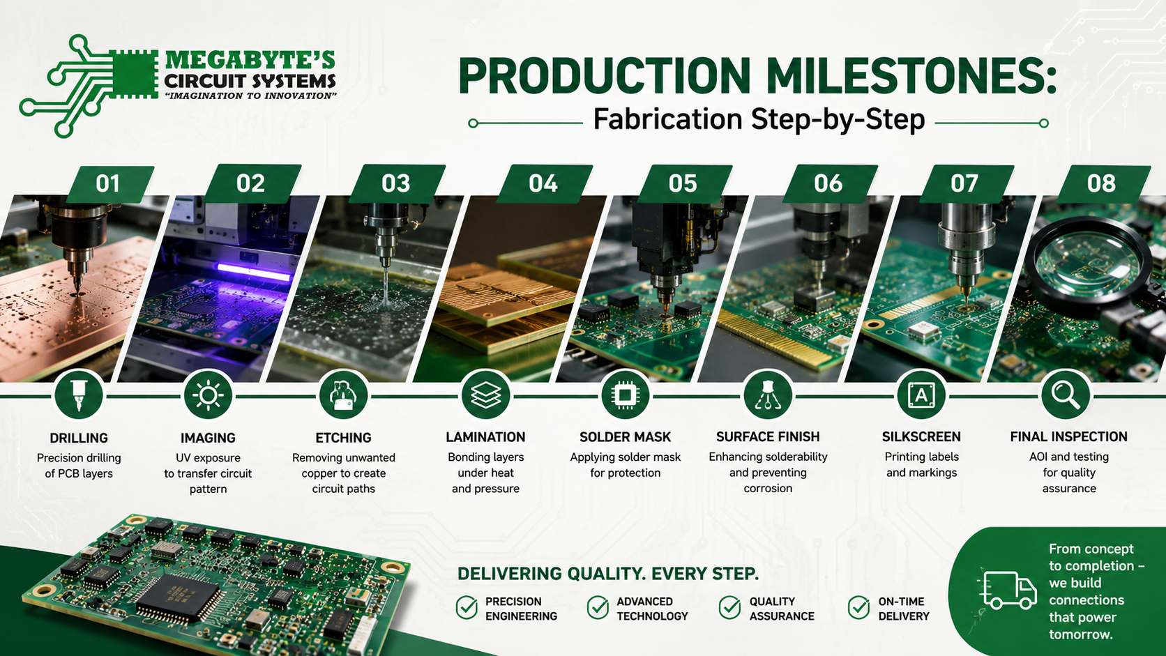
1.Material Cut and Inner Layer Preparation: Day 1.
Raw copper-clad FR-4 laminates are sheared to panel sizes. For a Multilayer PCB, inner layer cores are thoroughly cleaned, coated with photosensitive dry film, and exposed via high-precision Laser Direct Imaging (LDI) to define internal signal traces.
2.Chemical Etching and Lamination: Day 2.
Unwanted copper is chemically stripped away, leaving only the intended circuit paths. The inner layers are treated with an oxide coating to enhance adhesion, interleaved with prepreg (resin-impregnated fiberglass), and compressed under intense hydraulic pressure and heat to form a solid monolithic structure.
3.CNC Drilling and Desmear: Day 3.
High-speed CNC drilling machines drill the structural and via holes through the panel. Frictional heat from drilling can melt resin inside the holes, creating an insulative “resin smear.” Panels undergo a chemical desmear process to clean the copper interconnect faces before plating.
4.Electroless Copper Plating & Outer Layer Imaging: Day 3-4.
A micro-thin layer of copper is chemically deposited along the non-conductive barrel walls of the drilled holes through electroless plating. The outer layers are then imaged via LDI, followed by electrolytic electroplating to build outer layer traces and hole walls to their final required copper weight.
5.Solder Mask and Surface Finish Application: Day 4-5.
Liquid Photoimageable (LPI) solder mask whether standard green, high-visibility blue, or clean yellow is coated across the panel to protect copper traces from moisture and bridging. Exposed pads are treated with a surface finish like HASL (Hot Air Solder Leveling) or ENIG (Electroless Nickel Immersion Gold) to ensure excellent solderability during assembly.
When you are manufacturing electronics destined for commercial deployment or rugged industrial use, quality control cannot be an afterthought. Your supply chain strategy must include verifiable quality verification gating at every step of production.
At Megabyte Circuit Systems, we focus heavily on the globally recognized IPC-A-600 standard, which dictates acceptable visual and structural criteria for rigid printed circuit boards. Every single panel passing through production is subjected to strict test protocols:
Before multilayer lamination occurs, automated high-resolution optical scanning systems compare the etched copper layers against your original Gerber vector data. This stage catches microscopic hair-line opens or copper mouse-bites that no human eye could spot under a magnifying lamp.
Every bare board must face a dedicated electrical validation sequence before packaging. For high-volume production, customized hard-wired bed-of-nails fixtures test every net simultaneously.
For small-to-medium batches and quick-turn prototyping, automated flying probe testers move high-speed test pins rapidly across the board surface to verify continuity and check for unintended shorts down to fractional ohm tolerances.
For high-speed communication interfaces like USB 3.0, HDMI, or differential DDR memory buses, matching signal line impedance is critical to prevent signal reflections and data degradation.
We use advanced polar instruments and tightly controlled trace-to-plane stackups to guarantee your target trace impedance requirements (e.g., $50\,\Omega$ single-ended or $90\,\Omega$/$100\,\Omega$ differential pairs) stay within a $\pm10\%$ window.
Quick Technical Summary: Adherence to IPC-A-600 standards combined with 100% AOI and flying probe testing eliminates field failures. Controlled impedance validations guarantee signal integrity for modern high-speed microprocessors and RF communications.
A perfectly fabricated bare board is just half the battle. To bring a product to life, it must pass through an automated PCB Assembly service. If you do not actively monitor component sourcing, your production timelines will inevitably slip due to single-source component shortages.
To optimize your Bill of Materials (BOM) sourcing for production within India, follow these direct sourcing rules:
Managing production overhead while scaling a product in India comes down to subtle geometry decisions and freight logistics. You do not need to cut corners on material quality to achieve competitive unit pricing; instead, optimize how your design interfaces with factory panelization.
PCB manufacturing is priced by the total square area of the panels processed. If your board has an irregular shape (L-shaped, circular, or jagged edges), placing those boards into a rectangular matrix leaves significant unused copper that must be etched away.
Working closely with our engineering team allows you to implement smart panel arrays with tab-routing or V-scores, packing more functional units into every single panel and driving down per-board costs.
Ensure your layout maintains a relatively balanced distribution of copper between the top and bottom layers. Drastic differences in copper density between layers cause uneven stress distribution across the FR-4 laminate during thermal processing, leading to structural bowing or twisting after wave soldering.
Additionally, unless your design absolutely requires four layers for complex routing planes, designing a highly optimized Double Layer PCB offers excellent electrical routing capacity at a fraction of the cost.
Choosing an established domestic manufacturing partner eliminates unpredictable international air freight fees, complex import customs clearances, and unexpected currency fluctuations. Operating out of our modern facility in Ahmedabad, Gujarat, we ensure clear technical communication, direct engineering alignment, and rapid logistics options across major Indian industrial hubs.
For standard quick-turn prototyping (single or double-layer), fabrication typically takes between 3 to 5 business days. For complex multilayer production runs requiring advanced lamination and electrical profiling, typical manufacturing lead times range from 10 to 15 business days depending on volume and component sourcing.
For rugged industrial deployments facing ambient humidity and thermal variations, ENIG (Electroless Nickel Immersion Gold) is highly recommended. It offers a perfectly flat surface for fine-pitch SMT placement, excellent oxidation resistance, and long-term shelf life. For cost-conscious consumer hardware or simpler assemblies, lead-free HASL (Hot Air Solder Leveling) is an excellent, reliable alternative.
Standard boards utilize $1\,\text{oz}$ copper ($35\,\mu\text{m}$ thickness). Specifying heavy copper paths ($2\,\text{oz}$ to $3\,\text{oz}$) for high-current power boards requires longer chemical etching times, specialized lamination steps to handle the deeper track profiles, and carries a material cost premium.
IoT hardware often integrates tight RF layout sections, high-density BGAs, and compact form factors. A comprehensive upfront DFM check verifies that trace shielding geometry, via pad clearances, and layer stackups prevent cross-talk and fabrication defects before copper panels are cut, preventing scrap material and layout revisions.
Yes. As long as you provide standard, industry-compliant Gerber files (RS-274X or Extended ODB++), along with IPC-compliant NC Drill files and an accurate layer stackup definition, a professional domestic facility can seamlessly configure its manufacturing lines to match your exact design parameters.
Navigating the transition from layout to physical product does not have to be an uphill battle against uncoordinated suppliers and unpredictable quality. By aligning your design principles with proven DFM guidelines, selecting locally stocked materials, and working with a partner committed to rigorous quality control, you can build a stable, scalable production pipeline.
At Megabyte Circuit Systems, based in Ahmedabad, Gujarat, we provide comprehensive, end-to-end support for your hardware roadmap. From quick-turn multi-layer prototyping to high-volume commercial production, our team ensures your designs are built to international IPC standards and delivered exactly when you need them.
Are you preparing to scale your next hardware project? Bring your engineering and procurement teams into alignment today. Use our intuitive online PCB Calculator to estimate project costs, explore our specialized engineering capabilities, or reach out to our consulting desk directly at quote@megabytecircuit.com to secure a comprehensive technical quote for your Gerber files.
C/10, Yogeshwar Estate, B/H Madhuram Estate, Nr. Vishala Estate, Sardar Patel Ring Rd, Odhav, Ahmedabad, Gujarat, Ahmedabad - 382430, Gujarat (India)
Copyright © 2025. Megabytes Circuit Systems All rights reserved.
Powered by FrogMEE Tech