Ahmedabad - 382430, Gujarat (India)
Moving from a functional desktop prototype to mass manufacturing thousands of units is the ultimate trial by fire for an electronics hardware team. In my 20+ years of engineering and plant management across India’s electronics clusters, I’ve seen hundreds of brilliant designs choke at the scaling phase.
The culprit is rarely a lack of engineering talent; it is almost always a mismatch between the product’s requirements and the actual capability of the chosen factory partner.
When you scale to massive production runs, a minor defect rate of 0.5% that felt acceptable during prototyping scales into an absolute logistical nightmare of component rework, field failures, and smashed margins.
Finding the right pcb company in India isn’t just about scrolling through vendor listings or looking at the absolute lowest cost per board. It requires a meticulous deep dive into automated processes, material chain transparency, and local design validation support. Let’s break down exactly what you must look for in a Tier-1 hardware fabrication partner to ensure your high-volume deployment scales smoothly.
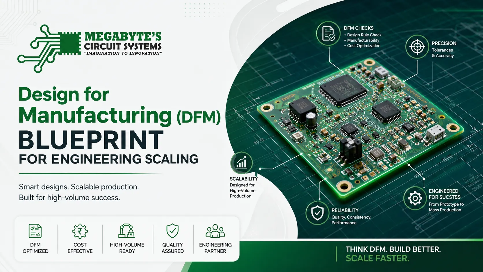
One thing I always tell my clients is that mass manufacturing optimization begins long before a single copper sheet is laminated. A true Tier-1 fabrication partner will never blindly drop your raw Gerber data into an automated etching bath.
They must possess a dedicated pre-production team that reviews your design data against physical factory constraints using sophisticated Design for Manufacturing (DFM) check suites.
We see this issue very often with hardware startups: an engineer sets tight multi-layer track clearances or micro-vias that easily passed the loose tolerances of a rapid prototyping shop, but become low-yield bottlenecks on a high-speed production line.
Your manufacturing partner needs to actively check trace widths, copper balance, annular rings, and solder mask expansion clear zones to prevent common defects like solder bridging or panel warpage during assembly.
High-volume electronics scaling requires a rigid automated Design for Manufacturing (DFM) verification to catch fabrication errors before panellization. Key pre-production focus points include strict trace width/spacing validation, copper density balancing across internal planes, and systematic aspect ratio checks for plated through-holes.
When evaluating a pcb company in India for sustained high-volume runs, you must look beyond their square-meter factory floor capacity and closely analyze their automation baseline. Manual testing or basic fixture-based sampling is totally insufficient when handling tens of thousands of complex multi-layer assemblies.
A high-tier facility must employ Automated Optical Inspection (AOI) after dry-film development and post-etching to trap pattern anomalies that human inspectors miss. Furthermore, look for internal infrastructure handling 100% netlist verification via high-speed flying probe testers or dedicated automated bed-of-nails fixture testing for dense production panels.
For critical industrial IoT, automotive control units, or medical equipment, material reliability under thermal duress is non-negotiable. You need absolute transparency regarding the exact laminates being stacked in the press. Tier-1 facilities operate strictly within global quality boundaries, maintaining certified compliance with IPC-A-600 (Acceptability of Printed Boards) Class 2 or Class 3 parameters alongside clean ISO 9001:2015 quality records.
Ask potential suppliers for their raw material tracking processes. Are they sourcing certified, flame-retardant FR-4 materials with a stable glass transition temperature ($T_g$) suited for lead-free automated reflow processes? High-volume manufacturing demands continuous panel-to-panel consistency, which is impossible if the factory mixes unbranded, low-grade laminates into production batches.
To paint a clear picture of why a high-volume scaling infrastructure differs from basic desktop prototyping houses, analyze this operational blueprint:
| Process / Attribute | Small-Batch Prototyping Baseline | High-Volume Tier-1 Production Standard |
| Primary Imaging Method | Laser Direct Imaging (LDI) / Proto Plotter | High-Throughput LDI paired with Automated Contact Photolithography |
| Electrical Validation | Flying Probe Testing (Flexible, slower turnaround per board) | Customized Bed-of-Nails Dedicated Fixture Testing (Rapid multi-point scan) |
| DFM Verification | Basic automated DRC check rules | Multi-stage, multi-layer matrix validation optimizing panelization layout |
| Quality Compliance | Manufacturer internal visual checks | Certified IPC-A-600 Class 2/3, UL Marking, and complete lot traceability |
| Laminate Controls | Standard commercial grade FR-4 sheets | Controlled $T_g$/$T_d$ tracking, matched copper thickness weights, multi-layer stack balance |
To avoid production interruptions at the factory gate, your engineering team should ensure your layout files align smoothly with high-volume industrial processing parameters. Below is a quick baseline checklist detailing production tolerances for standard multi-layer and high-density designs:
If your design incorporates high-speed differential signal transmission lines (such as USB 3.0, PCIe, or Ethernet links), trace width must be precisely calculated alongside dielectric thickness using the standard Microstrip differential characteristic impedance approximation formula:
Where:
A premium manufacturing partner will run an advanced field solver on your specific layer stackup configuration to fine-tune trace dimensions before production panels are generated.
High-speed high-volume PCB scaling mandates exact trace geometry and dielectric height monitoring to satisfy controlled impedance constraints. Mechanical drill aspect ratios must remain bounded within a $10:1$ ratio to guarantee completely uniform electroplating across all internal layers.
Managing long-term production costs when picking a manufacturing partner in India involves looking closely at panel utilization efficiency and local supply chains.
For high-volume multi-layer configurations, it is best to keep the aspect ratio at or below $10:1$. If you are running a standard $1.6\text{ mm}$ thick panel, your smallest drilled through-hole should not be lower than $0.2\text{ mm}$ to ensure complete chemical and copper plating coverage through the entire inner barrel.
Uneven or mismatched copper distribution between the top and bottom layers of a multi-layer board creates asymmetrical structural tension. When these boards travel through the intense heat of automated reflow ovens, this structural imbalance can cause severe board warping, twist defects, and broken surface-mount joints.
IPC Class 2 covers standard high-reliability industrial and commercial electronics where continuous operation is preferred but not life-critical. Class 3 imposes much tougher quality checks, requiring absolute zero-downtime performance with extra copper plating thickness inside through-holes, making it essential for medical life support and aerospace systems.
You should move to High-$T_g$ materials (typically greater than $170^\circ\text{C}$) if your hardware operates in sustained ambient temperatures exceeding $130^\circ\text{C}$, or if the circuit pattern features dense multi-layer routing that requires multiple back-to-back thermal reflow processing cycles.
Yes, during the pre-production DFM engineering phase, the manufacturing plant calculates real-world impedance using their specific material parameters. They will suggest slight trace modifications to match your target $50\Omega$ or $90\Omega$ requirements based on real-world factory lamination tolerances.
Scaling a high-volume hardware product demands an experienced fabrication partner that values technical precision over cut-rate shortcuts. Based in Ahmedabad, Gujarat, Megabyte Circuit Systems delivers cutting-edge, dependable industrial hardware production tailored specifically for Indian hardware innovators, Tier-1 industrial procurement procurement groups, and scaling IoT startups.
Whether your deployment needs a robust Single Layer PCB layout, high-performance Double Layer PCB routing, or ultra-dense, impedance-controlled Multilayer PCB stackups, our facility provides comprehensive support. We bridge the gap between design concepts and large-scale manufacturing realities by offering dedicated pre-production DFM verification, strict quality auditing, and fast local turnarounds.
Ready to transition your electronic architecture to full production scale? Skip the friction of international shipping delays and complex customs clearings. Get immediate, itemized factory pricing for your production batch by using our easy online PCB Calculator, or reach out directly to our engineering consulting desk to kickstart our specialized PCB Manufacturing service workflow today.
C/10, Yogeshwar Estate, B/H Madhuram Estate, Nr. Vishala Estate, Sardar Patel Ring Rd, Odhav, Ahmedabad, Gujarat, Ahmedabad - 382430, Gujarat (India)
Copyright © 2025. Megabytes Circuit Systems All rights reserved.
Powered by FrogMEE Tech